ADSP-2186
Bootstrap Loading (Booting)
The
However, three bits are used to ensure future compatibility with parts containing internal program memory ROM.
BDMA Booting
When the MODE pins specify BDMA booting, the
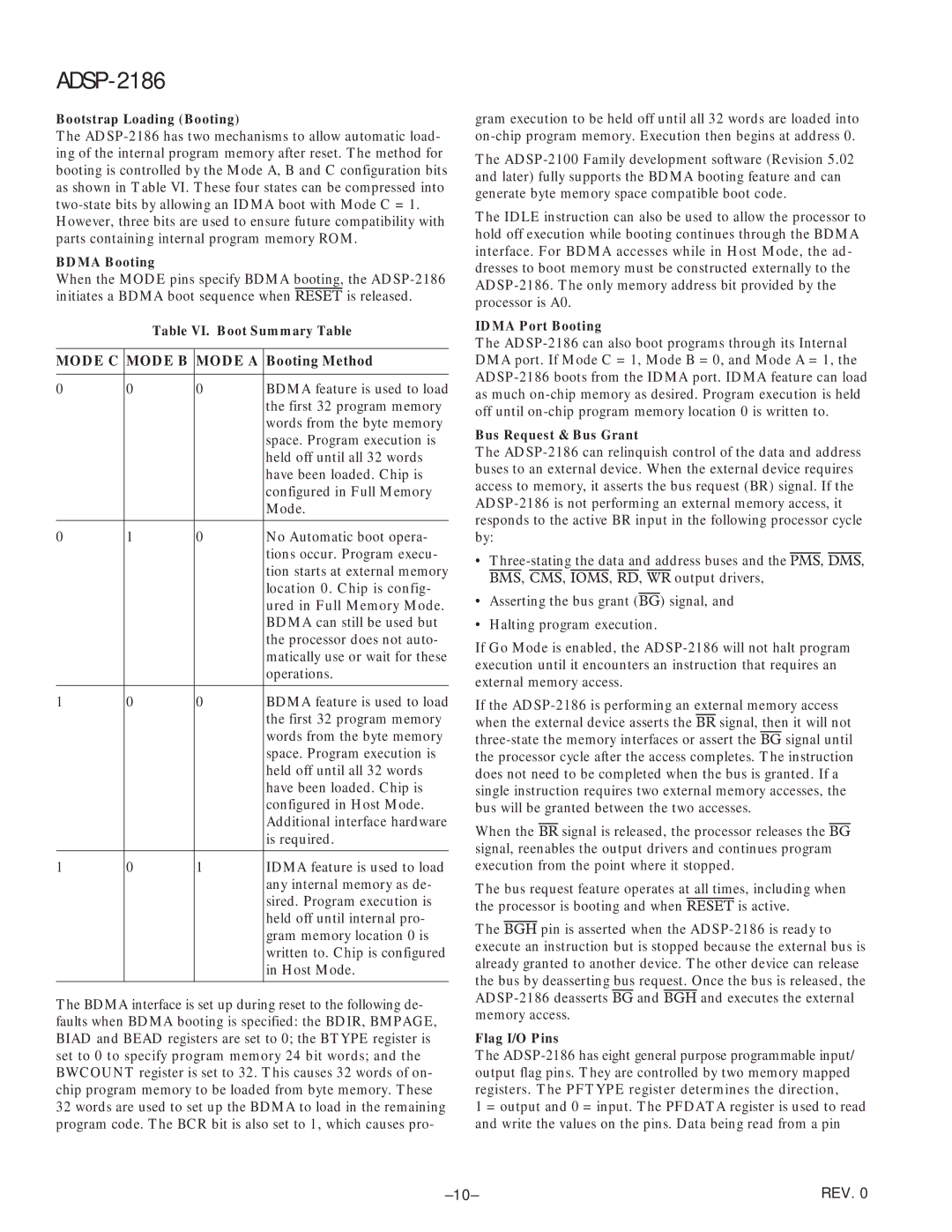
Table VI. Boot Summary Table
MODE C | MODE B | MODE A | Booting Method |
|
|
|
|
0 | 0 | 0 | BDMA feature is used to load |
|
|
| the first 32 program memory |
|
|
| words from the byte memory |
|
|
| space. Program execution is |
|
|
| held off until all 32 words |
|
|
| have been loaded. Chip is |
|
|
| configured in Full Memory |
|
|
| Mode. |
|
|
|
|
0 | 1 | 0 | No Automatic boot opera- |
|
|
| tions occur. Program execu- |
|
|
| tion starts at external memory |
|
|
| location 0. Chip is config- |
|
|
| ured in Full Memory Mode. |
|
|
| BDMA can still be used but |
|
|
| the processor does not auto- |
|
|
| matically use or wait for these |
|
|
| operations. |
|
|
|
|
1 | 0 | 0 | BDMA feature is used to load |
|
|
| the first 32 program memory |
|
|
| words from the byte memory |
|
|
| space. Program execution is |
|
|
| held off until all 32 words |
|
|
| have been loaded. Chip is |
|
|
| configured in Host Mode. |
|
|
| Additional interface hardware |
|
|
| is required. |
|
|
|
|
1 | 0 | 1 | IDMA feature is used to load |
|
|
| any internal memory as de- |
|
|
| sired. Program execution is |
|
|
| held off until internal pro- |
|
|
| gram memory location 0 is |
|
|
| written to. Chip is configured |
|
|
| in Host Mode. |
|
|
|
|
The BDMA interface is set up during reset to the following de- faults when BDMA booting is specified: the BDIR, BMPAGE, BIAD and BEAD registers are set to 0; the BTYPE register is set to 0 to specify program memory 24 bit words; and the BWCOUNT register is set to 32. This causes 32 words of on- chip program memory to be loaded from byte memory. These 32 words are used to set up the BDMA to load in the remaining program code. The BCR bit is also set to 1, which causes pro-
gram execution to be held off until all 32 words are loaded into
The
The IDLE instruction can also be used to allow the processor to hold off execution while booting continues through the BDMA interface. For BDMA accesses while in Host Mode, the ad- dresses to boot memory must be constructed externally to the
IDMA Port Booting
The
Bus Request & Bus Grant
The
•
•Asserting the bus grant (BG) signal, and
•Halting program execution.
If Go Mode is enabled, the
If the
When the BR signal is released, the processor releases the BG signal, reenables the output drivers and continues program execution from the point where it stopped.
The bus request feature operates at all times, including when the processor is booting and when RESET is active.
The BGH pin is asserted when the
Flag I/O Pins
The
1 = output and 0 = input. The PFDATA register is used to read and write the values on the pins. Data being read from a pin
REV. 0 |