Contents
Functional Block Diagram
General Note
General Description
Development System
Additional Information
Architecture Overview
PIN Descriptions
Serial Ports
Common-Mode Pins
Input Pin Name Pins Output Function
Memory Interface Pins
Setting Memory Mode
Power-Down
LOW Power Operation
Source Of Interrupt Interrupt Vector Address Hex
Interrupts
Idle
Idle n
Slow Idle
System Interface
Reset
Clock Signals
Memory Architecture
Program Memory
Memory A13 A120
Space Full Memory Mode
Address Range Wait State Register
Data Memory
Internal Memory DMA Port Idma Port Host Memory Mode
Byte Memory DMA BDMA, Full Memory Mode
Internal
Memory Space Word Size Alignment
Booting Method
Syntax IOaddr = dreg dreg = IOaddr
MR Value Biased Unbiased Before RND RND Result
Biased Rounding
Designing AN EZ-ICE*-COMPATIBLE System
Target System Interface Signals
Target Board Connector for EZ-ICE* Probe
Target Memory Interface
PM, DM, BM, IOM, & CM
Grades Parameter Test Conditions Min Typ Max Unit
Grade Parameter Min Max Unit
WR Low
Power Dissipation
Total Power Dissipation = Pint + C × VDD2 × f
Package
Assumptions
Output Enable Time
Output Disable Time
Capacitive Loading
Test Conditions
Control Signals
Parameter Min Max Clock Signals and Reset
Flag Output Delay from Clkout Low5 TCK +
IRQx FI, or PFx Setup before Clkout Low1, 2, 3 TCK +
Parameter Min Max Unit Interrupts and Flag
Flag Output Hold after Clkout Low5 25 tCK
Parameter Min Max Unit Bus Request/Grant
Parameter Min Max Unit Memory Read
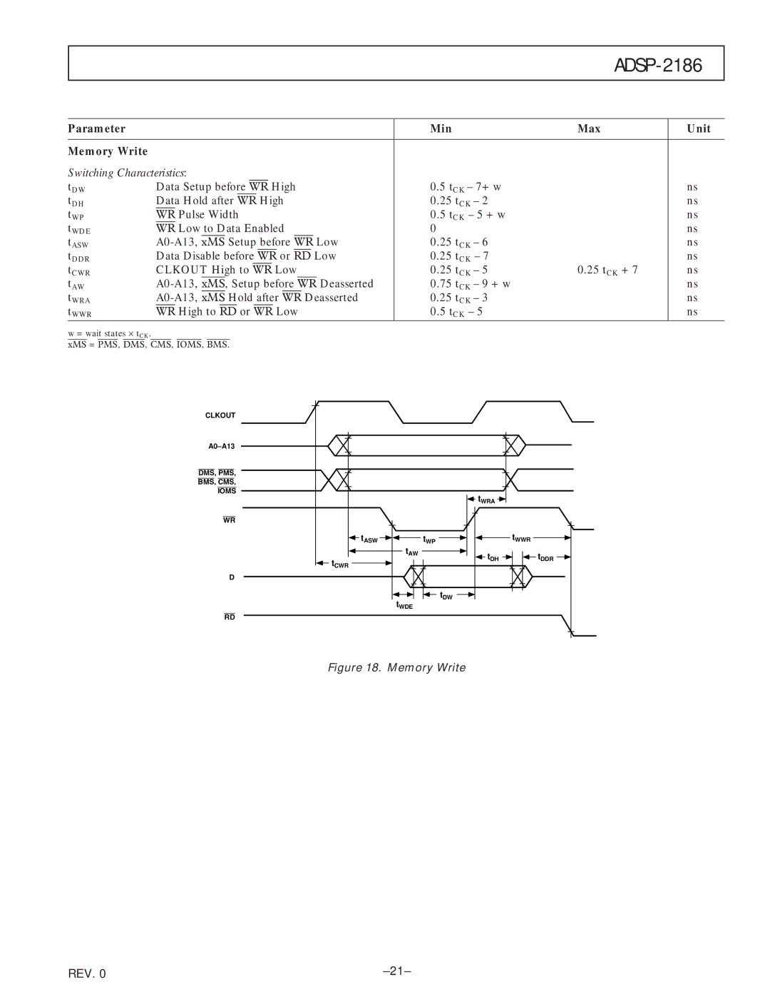
Parameter Min Max Unit Memory Write
Parameter Min Max Unit Serial Ports
Parameter Min Max Unit Idma Address Latch
Parameter Min Max Idma Write, Short Write Cycle
IAD15-0 Data Setup before End of Write2, 3
Iack Low before Start of Write1
Duration of Write1
Parameter Min Max Unit Idma Write, Long Write Cycle
IAD15-0 Data Setup before
Low before Start of Write1
Low4 TCK
Parameter Min Max Unit Idma Read, Long Read Cycle
Duration of Read Switching Characteristics
Parameter Min Max Unit Idma Read, Short Read Cycle
High after Start of Read1
ADSP-2186
Lead Tqfp Package Pinout
Number Name A4/IAD3
Pin
A5/IAD4
A6/IAD5
Outline Dimensions
Ordering Guide
ST-100
Page
C2999-6-3/97