a
DSP Microcomputer
ADSP-2186
FEATURES PERFORMANCE
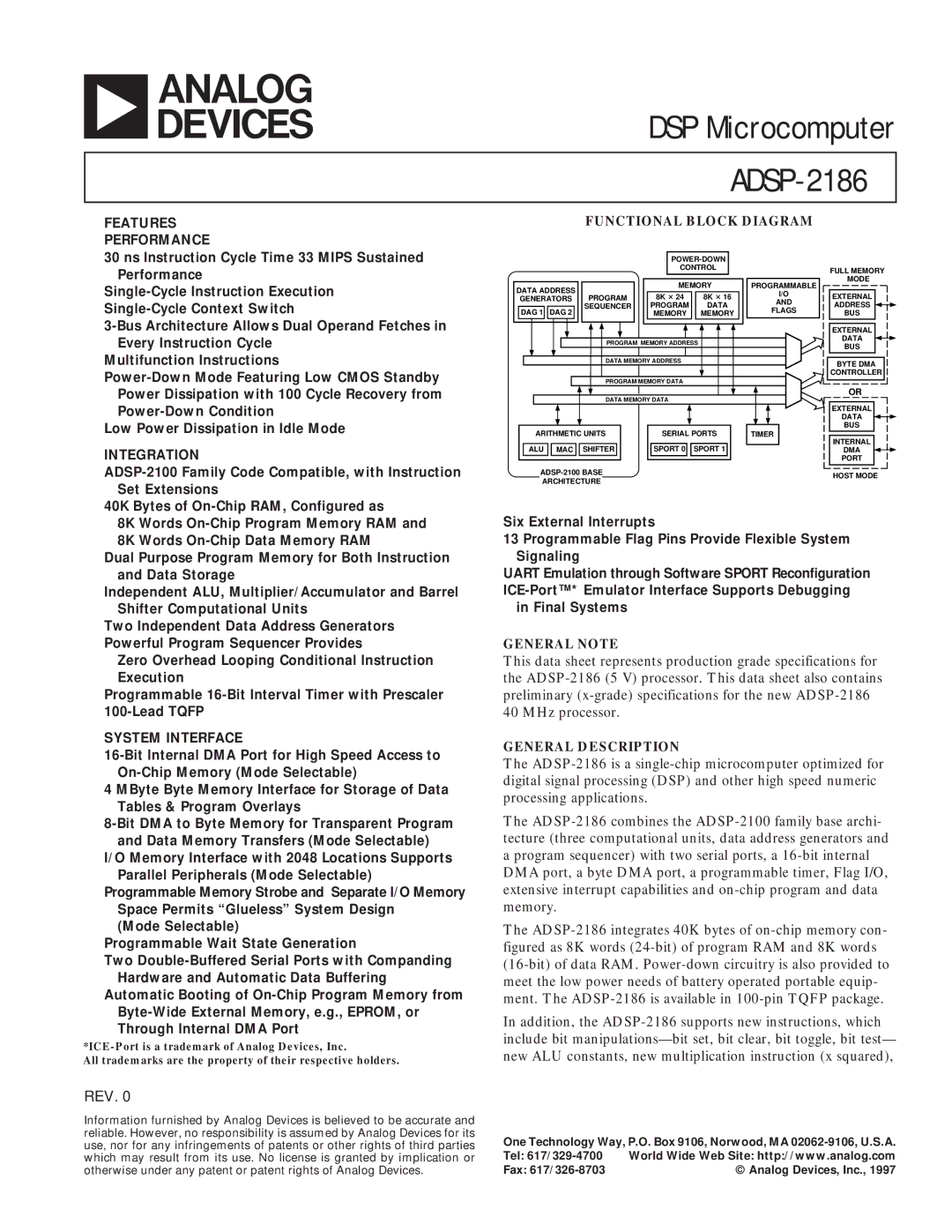
FUNCTIONAL BLOCK DIAGRAM
30 ns Instruction Cycle Time 33 MIPS Sustained Performance
Multifunction Instructions
Low Power Dissipation in Idle Mode
INTEGRATION
40K Bytes of
|
|
|
|
|
|
|
|
|
|
|
|
| ||||
|
|
|
|
|
|
|
|
|
| CONTROL |
|
|
| |||
|
|
|
|
|
|
|
|
|
|
|
|
|
|
|
|
|
|
|
|
|
|
|
|
|
|
|
|
|
|
|
|
|
|
DATA ADDRESS |
|
|
|
|
| MEMORY |
| PROGRAMMABLE | ||||||||
|
|
|
|
|
|
|
|
|
|
| I/O | |||||
| GENERATORS |
| PROGRAM |
|
| 8K 24 |
| 8K 16 |
|
| AND | |||||
|
|
|
|
|
| SEQUENCER |
|
| PROGRAM |
| DATA |
|
| |||
| DAG 1 |
| DAG 2 |
|
|
|
|
| MEMORY |
| MEMORY |
|
| FLAGS | ||
|
|
|
|
|
|
|
|
|
|
|
|
|
|
|
|
|
PROGRAM MEMORY ADDRESS |
DATA MEMORY ADDRESS |
PROGRAM MEMORY DATA |
DATA MEMORY DATA
| ARITHMETIC UNITS |
|
| SERIAL PORTS |
| TIMER | ||||||||
|
|
|
|
|
|
|
|
|
|
|
|
|
|
|
| ALU |
| MAC |
| SHIFTER |
|
|
| SPORT 0 |
| SPORT 1 |
|
|
|
|
|
|
|
|
|
|
|
|
|
|
|
|
|
|
ARCHITECTURE
FULL MEMORY
MODE
EXTERNAL ADDRESS ![]()
![]()
BUS
EXTERNAL DATA ![]()
![]() BUS
BUS
BYTE DMA
CONTROLLER
OR
EXTERNAL DATA ![]()
![]()
![]() BUS
BUS
INTERNAL
DMA
PORT
HOST MODE
8K Words
8K Words
Dual Purpose Program Memory for Both Instruction and Data Storage
Independent ALU, Multiplier/Accumulator and Barrel Shifter Computational Units
Two Independent Data Address Generators Powerful Program Sequencer Provides
Zero Overhead Looping Conditional Instruction Execution
Programmable
SYSTEM INTERFACE
4 MByte Byte Memory Interface for Storage of Data Tables & Program Overlays
I/O Memory Interface with 2048 Locations Supports Parallel Peripherals (Mode Selectable)
Programmable Memory Strobe and Separate I/O Memory Space Permits “Glueless” System Design
(Mode Selectable)
Programmable Wait State Generation
Two
Automatic Booting of
All trademarks are the property of their respective holders.
REV. 0
Information furnished by Analog Devices is believed to be accurate and reliable. However, no responsibility is assumed by Analog Devices for its use, nor for any infringements of patents or other rights of third parties which may result from its use. No license is granted by implication or otherwise under any patent or patent rights of Analog Devices.
Six External Interrupts
13 Programmable Flag Pins Provide Flexible System Signaling
UART Emulation through Software SPORT Reconfiguration
in Final Systems
GENERAL NOTE
This data sheet represents production grade specifications for the
GENERAL DESCRIPTION
The
The
The
In addition, the
One Technology Way, P.O. Box 9106, Norwood, MA
Tel: | World Wide Web Site: http://www.analog.com |
Fax: | © Analog Devices, Inc., 1997 |