ADSP-2186
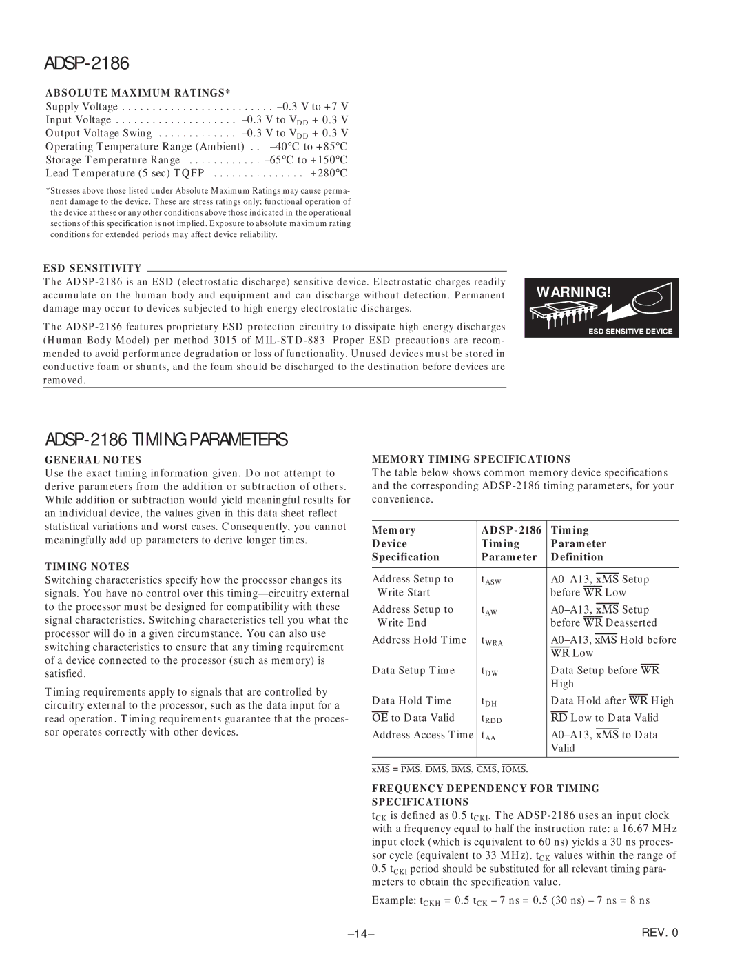
ABSOLUTE MAXIMUM RATINGS*
Supply Voltage . . . . . . . . . . . . . . . . . . . . . . . . .
Input Voltage . . . . . . . . . . . . . . . . . . . .
Output Voltage Swing . . . . . . . . . . . . .
Operating Temperature Range (Ambient) . .
Storage Temperature Range . . . . . . . . . . . .
Lead Temperature (5 sec) TQFP . . . . . . . . . . . . . . . +280°C
*Stresses above those listed under Absolute Maximum Ratings may cause perma- nent damage to the device. These are stress ratings only; functional operation of the device at these or any other conditions above those indicated in the operational sections of this specification is not implied. Exposure to absolute maximum rating conditions for extended periods may affect device reliability.
ESD SENSITIVITY
The
The
WARNING!
ESD SENSITIVE DEVICE
ADSP-2186 TIMING PARAMETERS
GENERAL NOTES
Use the exact timing information given. Do not attempt to derive parameters from the addition or subtraction of others. While addition or subtraction would yield meaningful results for an individual device, the values given in this data sheet reflect statistical variations and worst cases. Consequently, you cannot meaningfully add up parameters to derive longer times.
TIMING NOTES
Switching characteristics specify how the processor changes its signals. You have no control over this
Timing requirements apply to signals that are controlled by circuitry external to the processor, such as the data input for a read operation. Timing requirements guarantee that the proces- sor operates correctly with other devices.
MEMORY TIMING SPECIFICATIONS
The table below shows common memory device specifications and the corresponding
Memory | Timing | |
Device | Timing | Parameter |
Specification | Parameter | Definition |
|
|
|
Address Setup to | tASW | |
Write Start |
| before WR Low |
Address Setup to | tAW | |
Write End |
| before WR Deasserted |
Address Hold Time | tWRA | |
|
| WR Low |
Data Setup Time | tDW | Data Setup before WR |
|
| High |
Data Hold Time | tDH | Data Hold after WR High |
OE to Data Valid | tRDD | RD Low to Data Valid |
Address Access Time | tAA | |
|
| Valid |
|
|
|
xMS = PMS, DMS, BMS, CMS, IOMS.
FREQUENCY DEPENDENCY FOR TIMING
SPECIFICATIONS
tCK is defined as 0.5 tCKI. The
input clock (which is equivalent to 60 ns) yields a 30 ns proces- sor cycle (equivalent to 33 MHz). tCK values within the range of
0.5tCKI period should be substituted for all relevant timing para- meters to obtain the specification value.
Example: tCKH = 0.5 tCK – 7 ns = 0.5 (30 ns) – 7 ns = 8 ns
REV. 0 |
