ENVIRONMENTAL CONDITIONS |
|
|
| |||
Ambient Temperature Rating: |
|
|
| |||
TAMB | = TCASE – (PD x θCA) |
|
|
| ||
TCASE | = Case Temperature in °C |
| ||||
PD | = Power Dissipation in W |
|
|
| ||
θCA | = | Thermal Resistance |
| |||
θJA | = | Thermal Resistance | ||||
θJC | = | Thermal Resistance |
| |||
|
|
|
|
|
|
|
Package |
| uJA |
| uJC |
| uCA |
TQFP |
| 50°C/W |
| 2°C/W |
| 48°C/W |
|
|
|
|
|
|
|
POWER DISSIPATION
To determine total power dissipation in a specific application, the following equation should be applied for each output:
C× VDD2 × f
C = load capacitance, f = output switching frequency.
Example
In an application where external data memory is used and no other outputs are active, power dissipation is calculated as follows:
Assumptions
•External data memory is accessed every cycle with 50% of the address pins switching.
•External data memory writes occur every other cycle with 50% of the data pins switching.
•Each address and data pin has a 10 pF total load at the pin.
•The application operates at VDD = 5.0 V and tCK = 30 ns.
Total Power Dissipation = PINT + (C × VDD2 × f)
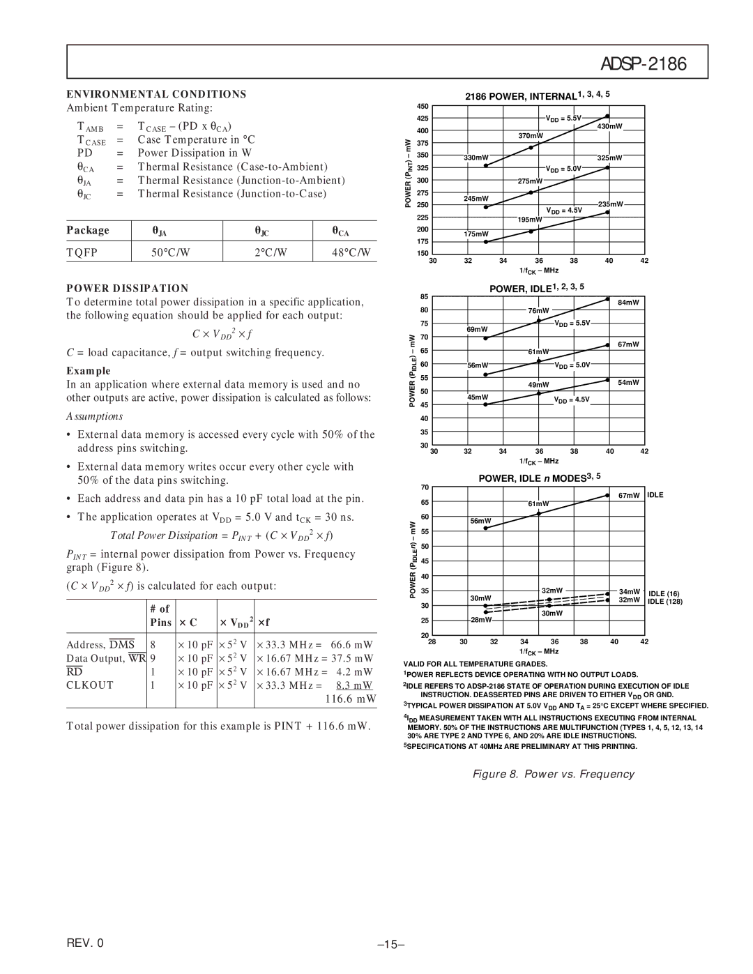
PINT = internal power dissipation from Power vs. Frequency graph (Figure 8).
(C × VDD2 × f) is calculated for each output:
| # of |
| 3 VDD2 |
|
| |
| Pins | 3 C | 3f |
| ||
|
|
|
|
|
|
|
Address, DMS | 8 | × 10 pF | × 52 | V | × 33.3 MHz = | 66.6 mW |
Data Output, WR | 9 | × 10 pF | × 52 | V | × 16.67 MHz = 37.5 mW | |
RD | 1 | × 10 pF | × 52 | V | × 16.67 MHz = | 4.2 mW |
CLKOUT | 1 | × 10 pF | × 52 | V | × 33.3 MHz = | 8.3 mW |
|
|
|
|
| 116.6 mW | |
|
|
|
|
|
|
|
Total power dissipation for this example is PINT + 116.6 mW.
|
|
| ||
| 450 | 2186 POWER, INTERNAL1, 3, 4, 5 | ||
|
|
| ||
| 425 |
| VDD = 5.5V | |
| 400 |
| 430mW | |
|
| 370mW | ||
– mW | 375 |
| ||
|
| |||
350 | 330mW | 325mW | ||
) |
| |||
INT | 325 |
| VDD = 5.0V | |
(P | 300 |
| 275mW | |
POWER |
| |||
275 | 245mW |
| ||
250 | 235mW | |||
| ||||
| 225 |
| VDD = 4.5V | |
|
| 195mW | ||
| 200 | 175mW |
| |
| 175 |
| ||
|
|
| ||
| 150 |
|
| |
| 30 | 32 | 34 | 36 | 38 | 40 | 42 |
|
|
|
| 1/fCK – MHz |
|
| |
| 85 |
| POWER, IDLE1, 2, 3, 5 |
|
| ||
|
|
|
|
|
| 84mW | |
| 80 |
|
| 76mW |
|
| |
|
|
|
|
|
| ||
| 75 | 69mW |
|
| VDD = 5.5V |
|
|
– mW | 70 |
|
|
|
|
| |
|
|
|
|
| 67mW | ||
65 |
|
| 61mW |
|
| ||
|
|
|
|
| |||
) |
|
|
|
|
|
|
|
IDLE | 60 | 56mW |
|
| VDD = 5.0V |
|
|
(P | 55 |
|
|
|
|
| 54mW |
POWER |
|
| 49mW |
|
| ||
|
|
|
|
| |||
50 |
|
|
|
|
| ||
45mW |
|
| VDD = 4.5V |
|
| ||
45 |
|
|
|
| |||
|
|
|
|
|
| ||
| 40 |
|
|
|
|
|
|
| 35 |
|
|
|
|
|
|
| 30 | 32 | 34 | 36 | 38 | 40 | 42 |
| 30 | ||||||
|
|
|
| 1/fCK – MHz |
|
| |
| 70 |
| POWER, IDLE n MODES3, 5 |
|
| |||
|
|
|
|
|
| 67mW | IDLE | |
| 65 |
|
| 61mW |
| |||
|
|
|
|
|
| |||
mW | 60 |
| 56mW |
|
|
|
|
|
|
|
|
|
|
|
| ||
55 |
|
|
|
|
|
|
| |
n) – | 50 |
|
|
|
|
|
|
|
IDLE |
|
|
|
|
|
|
| |
(P | 45 |
|
|
|
|
|
|
|
POWER | 35 |
|
|
| 32mW |
| 34mW | IDLE (16) |
| 40 |
|
|
|
|
|
|
|
| 30 |
| 30mW |
|
|
| 32mW | IDLE (128) |
|
|
|
| 30mW |
|
|
| |
| 25 |
| 28mW |
|
|
|
| |
|
|
|
|
|
|
| ||
| 20 | 30 | 32 | 34 | 36 | 38 | 40 | 42 |
| 28 | |||||||
|
|
|
| 1/fCK – MHz |
|
|
| |
VALID FOR ALL TEMPERATURE GRADES.
1POWER REFLECTS DEVICE OPERATING WITH NO OUTPUT LOADS.
2IDLE REFERS TO
3TYPICAL POWER DISSIPATION AT 5.0V VDD AND TA = 25°C EXCEPT WHERE SPECIFIED.
4IDD MEASUREMENT TAKEN WITH ALL INSTRUCTIONS EXECUTING FROM INTERNAL MEMORY. 50% OF THE INSTRUCTIONS ARE MULTIFUNCTION (TYPES 1, 4, 5, 12, 13, 14 30% ARE TYPE 2 AND TYPE 6, AND 20% ARE IDLE INSTRUCTIONS.
5SPECIFICATIONS AT 40MHz ARE PRELIMINARY AT THIS PRINTING.
Figure 8. Power vs. Frequency
REV. 0 |