Troubleshooting Guide
Fault Isolation Procedures
General Warnings
Suggested Tools
Related Publications
Symptom Tests
Introduction
Pretests
Component and System Codes
Diagnostic Procedure
YES
Fault Code Retrieval and Clearing
Service Procedure
Fault Code Isolation Procedure Index
Fault Hand-Held Codes
Driving Techniques
Right Turn Signal System Key on. If the fault is present,
Heat and vibration Brake Input Signal System
On. Apply Service Brake For Minimum Seconds. If
Speed Input Signal System
Seconds to set this fault
Description Type of Code Driving Technique 250
Symptom-Driving Index
Fault Isolation Procedures Service Procedure
Electrical Pretest
Overview
Step a
Electrical Pretest
Key off Disconnect negative battery cable
Step B
Measure resistance
Step C
Power-Up Sequence Test
Central Processing Unit Driver Display Unit Vehicle Harness
Central
Driver
Power-Up Sequence Test
Key on Observe the Driver If lights turn on the go off
If lights turn on and stay on
Freightliner IDI Measure voltage If voltage is between
Measure resistance between
If any of the above conditions are not met Go to Step D
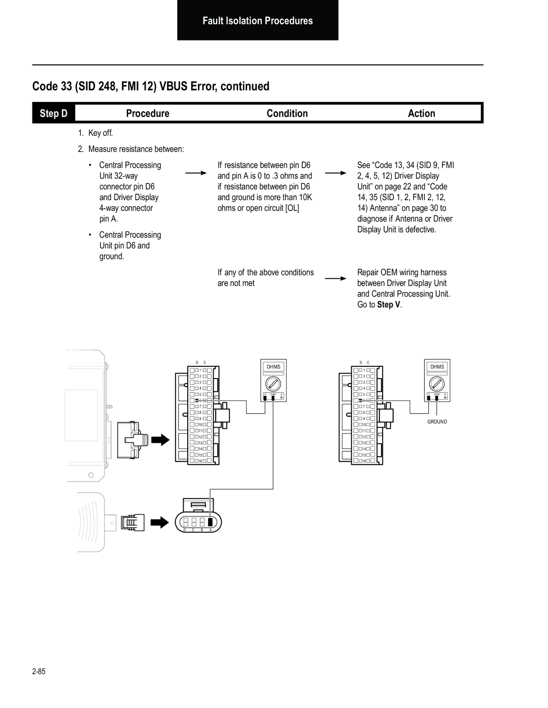
Step D
Key off Measure resistance between
If any of the above conditions are not met Go to Step E
Step E
If any of the above conditions are not met Go to Step F
Step F
If any of the above conditions are not met Go to Step G
Antenna 4-way connector
Step G
Step H
Step
Measure resistance between Central Processing
Are not met
Go to Step J
Step J
Key on Check error codes If no error codes
If error codes
Step K
Go to Step L
If error codes Go to Step a Find error in testing
Step L
Key off Reconnect all connectors Key on
Compatibility problem Contact your Bendix Representative
Check for Codes. See If no codes Test complete
Clearing on If code appears
This page left blank intentionally
Basic Hand Tools Troubleshooting Guide
Component Code 11 SID 254, FMI 4 Central Processing Unit CPU
Code 11, 12 SID 254, FMI 4, 12, Central Processing Unit CPU
Key off Retrieve codes If code 11 is active
If code 11 is inactive Test complete
This fault causes a failure of the Bendix Vorad system
Component Code 13 SID 9, FMI 2, 4, 5 Driver Display Unit
Code 13, 34 SID 9, FMI 2, 4, 5, 12 Driver Display Unit
Available, go to Step B Go to Step
If voltage is 7.0 to 7.5 volts
Driver Display Unit 4-way
Step C
5,12
Key off Measure resistance between Central Processing
Step E
Repair OEM wiring harness
Unit. Go to Step
Testing
Appears Procedure Index on
Clearing on page 1 If code 13 or 34 appears
If code other than 13 or
Component Code 14 SID 1, 2, FMI 2, 12 Antenna Assembly
Key off Unplug the Antenna 4-way connector Key on
Code 14, 35 SID 1, 2, FMI 2, 12, 14 Antenna
Pin 3 and pin If voltage is outside of range
Step C
Step D
Step E
Step F
Go to Step
See Fault Code Isolation
Clearing on page 1 If code 14 appears
Component Code SID 10, FMI Right Side Sensor
Key on Measure voltage between Pins a and B Pins a and C
If voltage between pins a
Code 15 SID 10, FMI 2 Right Side Sensor
Right Side Sensor?
If resistance is outside of range Go to Step D
Measure resistance between Way pin C13 and 3-way pin B
If resistance is outside of range Go to Step E
Replace Central processing Unit. Go to Step
See Fault Code Isolation Procedure Index on page 1
Component Code SID 11, FMI Left Side Sensor
Code 16 SID 11, FMI 2 Left Side Sensor
Left Side Sensor?
If resistance is out of range Go to Step D
Measure resistance between Way pin D13 and 3-way pin B
If resistance is out of range Go to Step E
If resistance is out of range
Clearing on page 1 If code 16 appears
Index on page 1
Component Code SID 7, FMI Right Turn Signal
Right Central Processing Unit Turn Signal
Code 21 SID 7, FMI 2 Right Turn Signal
Repair OEM wiring harness as
If equipped with a Right Side Sensor
Required. Go to Step
Key off Turn on right turn signal
Volts of battery voltage
If voltage flashes within
If code other than 21 appears
Component Code SID 8, FMI Left Turn Signal
Left
Code 22 SID 8, FMI 2 Left Turn Signal
Key off Turn on left turn signal
If voltage measures within
If code other than 22 appears
Component Code SID 3, FMI Brake Input Error
This fault causes a failure of the Vorad system
Code 23 SID 3, FMI 2 Brake Input Error
Go to Step B If the brake lights are not
Working correctly Go to Step
Proper configuration
Check pin C9 on 32-way If there is a wire in C9
Connector If there is not a wire in C9
Key off Depress brake pedal
Check for Codes. See If no codes appear Test complete
Clearing on page 1 If code 23 appears
This page left blank intentionally
Component Code SID 6, FMI Speed Input Error
Code 24 SID 6, FMI 2 Speed Input Error
Unit 32-way connector Have pins in C10 and C11
If vehicle uses J-1939 or 1587 configuration
Between speed sensor Pins a and B
10K ohms or open circuit
Ohms
Clearing on page 1 If code 24 appears
Component Code 25 SID 231, FMI 2, 12 Cruise Signal Error
Terminating
Resistor
Way pin D7 and ground
If resistance is outside of range Go to Step B
See Engine OEM for PIN Location
See Engine OEM For PIN Location
Key off Measure resistance
Key off Reconnect engine ECU connector
Key on If error codes Problem exists with Engine ECU. Repair
If code other than 25 appears
This page left blank intentionally
Component Code SID 250, FMI Data Link Error
Code 31 SID 250, FMI 2 J-1587 Data Link Error
If resistance is outside of range Go to Step C
Key on If no communication errors
If communication errors
If code other than 31 appears
This page left blank intentionally
Component Code SID 248, FMI Vbus Error
Code 33 SID 248, FMI 12 Vbus Error
If any of the above conditions are not met Go to Step B
If any of the above conditions are not met Go to Step C
Connector pin D5
Driver Display
Step D
On page 1
Clearing on page 1 If code 33 appears
Symptom Isolation Procedures
Antenna Not Detecting Targets
Appropriate isolation Properly Go to Step a Procedure
Side Sensor Not Detecting Targets
Side Sensor Detection Test
Between pins 2
Key on Measure voltage
Go to Step D If voltage is outside of range
Measure resistance between Way pin C16
4-way pin
Way pin C16 Ground
Replace Side Sensor Display. Go to Step Go to Step E
Key off Measure resistance between Way pin C14
Way pin C14 Ground
Go to Step Go to Step F
Key off Measure resistance between Way pin C12
Way pin C12 Ground
Ground is more than
If resistance is outside
Step
Detection Test
There is no fallback mode for this symptom
Driver Card Not Reading
New Driver Card
Driver Card Detection Test
Bendix Vorad System Wiring Diagram
Appendix
Wiring Diagram
Eatonvorad
Fault Code Tree
Nvram