CY7C1381DV25, CY7C1381FV25 CY7C1383DV25, CY7C1383FV25

Maximum Ratings

Exceeding the maximum ratings may impair the useful life of the device. For user guidelines, not tested.

Storage Temperature

–65°C to +150°C

Ambient Temperature with


Power Applied

–55°C to +125°C

Supply Voltage on VDD Relative to GND

–0.3V to +3.6V

Supply Voltage on VDDQ Relative to GND

–0.3V to +VDD

DC Voltage Applied to Outputs

–0.5V to VDDQ + 0.5V

in Tri-State

DC Input Voltage

–0.5V to VDD + 0.5V

Current into Outputs (LOW)


20 mA

Static Discharge Voltage


> 2001V

(per MIL-STD-883, Method 3015)


Latch-up Current


> 200 mA

Operating Range


Range

Ambient Temperature

VDD

VDDQ

Commercial

0°C to +70°C

2.5V ± 5%

2.5V – 5%


to VDD

Industrial

–40°C to +85°C


Electrical Characteristics

Over the Operating Range [16, 17]

Parameter

Description

Test Conditions

Min.

Max.

Unit

VDD

Power Supply Voltage


2.375

2.625

V

VDDQ

IO Supply Voltage

for 2.5V IO


2.375

VDD

V

VOH

Output HIGH Voltage

for 2.5V IO, IOH = –1.0 mA


2.0


V

VOL

Output LOW Voltage

for 2.5V IO, IOL = 1.0 mA


0.4

V

V

IH

Input HIGH Voltage [16]

for 2.5V IO


1.7

V + 0.3V

V


DD


VIL

Input LOW Voltage [16]

for 2.5V IO


–0.3

0.7

V

IX

Input Leakage Current

GND VI VDDQ


–5

5

A


except ZZ and MODE


Input Current of MODE

Input = VSS


–30


A


Input = VDD


5

A


Input Current of ZZ

Input = VSS


–5


A


Input = VDD


30

A

IOZ

Output Leakage Current

GND VI VDD, Output Disabled


–5

5

A

IDD

VDD Operating Supply

VDD = Max., IOUT = 0 mA,

7.5-ns cycle, 133 MHz


210

mA


Current

f = fMAX = 1/tCYC


10-ns cycle, 100 MHz


175

mA

ISB1

Automatic CE

Max. VDD, Device Deselected,

7.5-ns cycle, 133 MHz


140

mA


Power Down

VIN VIH or VIN VIL, f = fMAX,


10-ns cycle, 100 MHz


120


Current—TTL Inputs

inputs switching


ISB2

Automatic CE

Max. VDD, Device Deselected,

All speeds


70

mA


Power Down

VIN VDD – 0.3V or VIN 0.3V,


Current—CMOS Inputs

f = 0, inputs static


ISB3

Automatic CE

Max. VDD, Device Deselected,

7.5-ns cycle, 133 MHz


130

mA


Power Down

VIN VDDQ – 0.3V or VIN 0.3V,


10-ns cycle, 100 MHz


110

mA


Current—CMOS Inputs

f = fMAX, inputs switching


ISB4

Automatic CE

Max. VDD, Device Deselected,

All speeds


80

mA


Power Down

VIN VDD – 0.3V or VIN 0.3V,


Current—TTL Inputs

f = 0, inputs static


Notes

16.Overshoot: VIH(AC) < VDD +1.5V (Pulse width less than tCYC/2), undershoot: VIL(AC) > –2V (Pulse width less than tCYC/2).

17.Tpower up: assumes a linear ramp from 0V to VDD(min.) within 200 ms. During this time VIH < VDD and VDDQ < VDD.

Document #: 38-05547 Rev. *E

Page 17 of 28

[+] Feedback

Page 17
Image 17
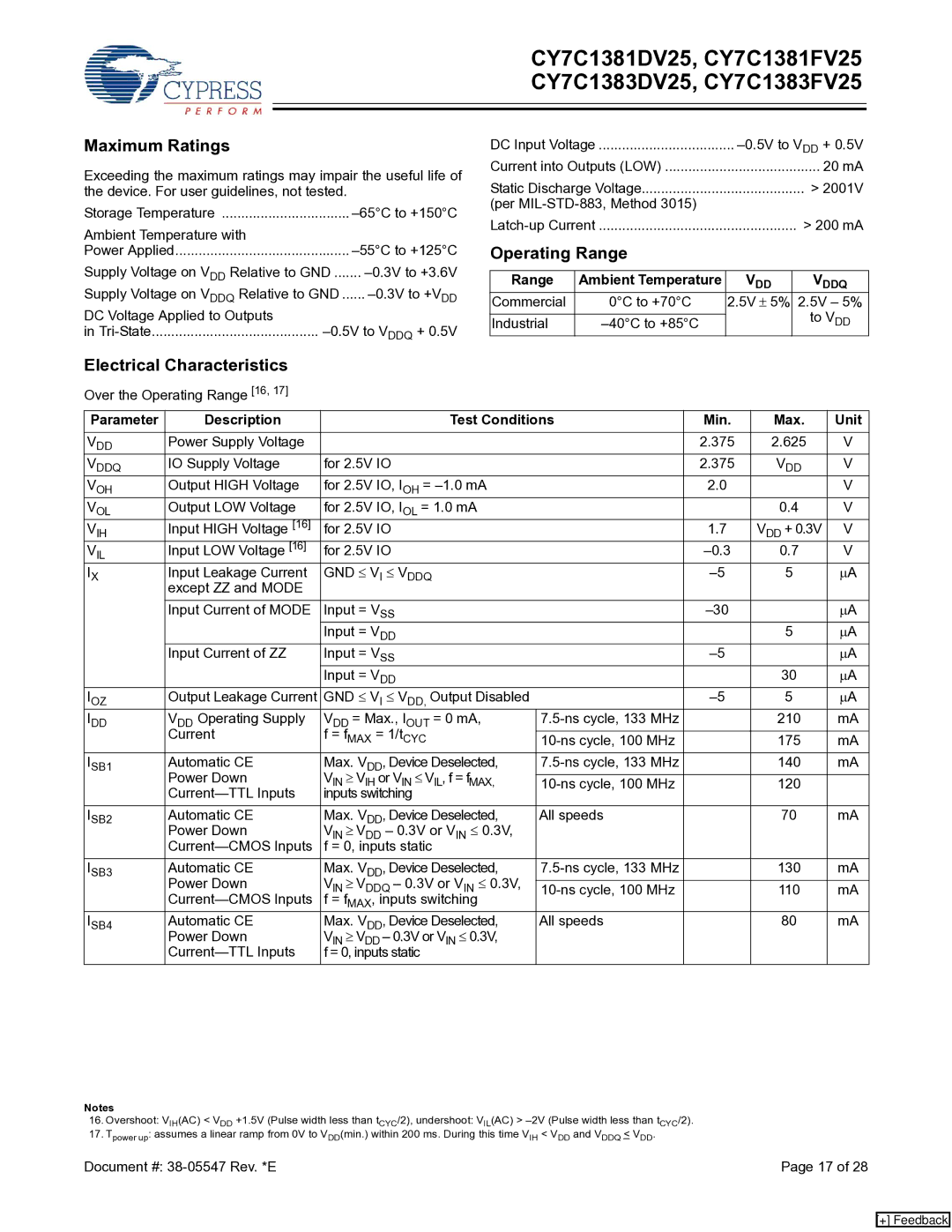
Cypress CY7C1381FV25, CY7C1383DV25 manual Maximum Ratings, Operating Range, Electrical Characteristics, GND ≤ VI ≤ Vddq

CY7C1383DV25, CY7C1381FV25, CY7C1381DV25, CY7C1383FV25 specifications

Cypress Semiconductor's family of static random-access memory (SRAM) chips, including the CY7C1381FV25, CY7C1383DV25, CY7C1381DV25, and CY7C1383FV25, are designed for high-performance applications that require fast access times and low power consumption. These devices are often found in applications such as networking, telecommunications, and industrial control systems, where speed and reliability are paramount.

The CY7C1381FV25 and CY7C1381DV25 are single-port SRAMs, while the CY7C1383FV25 and CY7C1383DV25 are dual-port versions that allow for simultaneous read and write operations from two different controllers. This feature significantly enhances data throughput, making these devices ideal for high-bandwidth applications. The devices support asynchronous read and write operations, ensuring immediate data accessibility with minimal latency.

One of the key features of these SRAM chips is their fast access times, with read and write cycles as short as 10 nanoseconds. This speed makes them suitable for cache memory applications, where performance is critical. Furthermore, the devices are built on Cypress's advanced process technology, which enables them to achieve high density and low power consumption, ideal for battery-operated devices and systems where energy efficiency is crucial.

The power consumption characteristics also highlight their effectiveness in various applications. The active power consumption can be as low as 80mA, depending on the operation conditions, and the devices offer low standby power, further enhancing their suitability for low-power applications. Additionally, these chips incorporate power-saving features like sleep mode, allowing designers to minimize energy consumption in idle states.

In terms of reliability, Cypress employs rigorous quality control measures, ensuring that the CY7C1381FV25, CY7C1383DV25, CY7C1381DV25, and CY7C1383FV25 meet stringent industry standards. They also feature an extended temperature range, which is vital for industrial applications that may experience harsh environmental conditions.

Overall, the CY7C1381FV25, CY7C1383DV25, CY7C1381DV25, and CY7C1383FV25 SRAM chips are versatile, high-performance memory solutions. Their combination of fast access times, low power consumption, and reliability makes them an excellent choice for engineers and developers looking to implement high-speed memory in a variety of applications. Whether for a communication device or a sophisticated industrial control system, these Cypress SRAMs stand out in the market for their performance and efficiency.