Features
CY7C1381DV25, CY7C1381FV25 CY7C1383DV25, CY7C1383FV25
Selection Guide
Functional Description
Logic Block Diagram - CY7C1381DV25/CY7C1381FV25 3 512K x
Logic Block Diagram - CY7C1383DV25/CY7C1383FV25 3 1M x
CY7C1381DV25, CY7C1381FV25
CY7C1383DV25, CY7C1383FV25
Pin Configurations 100-pin TQFP Pinout 3 Chip Enable
CY7C1381DV25, CY7C1381FV25 CY7C1383DV25, CY7C1383FV25
CY7C1381DV25
512K x
Pin Configurations continued 119-Ball BGA Pinout
CY7C1381FV25 512K x
CY7C1383FV25 1M x
CY7C1381DV25, CY7C1381FV25 CY7C1383DV25, CY7C1383FV25
Pin Configurations continued 165-Ball FBGA Pinout3 Chip Enable
CY7C1381DV25 512K x
CY7C1383DV25 1Mx
CY7C1381DV25, CY7C1381FV25 CY7C1383DV25, CY7C1383FV25
Pin Definitions
CY7C1381DV25, CY7C1381FV25 CY7C1383DV25, CY7C1383FV25
Name
Description
Pin Definitions continued
Functional Overview
CY7C1381DV25, CY7C1381FV25
CY7C1383DV25, CY7C1383FV25
ZZ Mode Electrical Characteristics
CY7C1381DV25, CY7C1381FV25 CY7C1383DV25, CY7C1383FV25
Interleaved Burst Address Table MODE = Floating or VDD
Address
CY7C1381DV25, CY7C1381FV25 CY7C1383DV25, CY7C1383FV25
Truth Table 4, 5, 6, 7
Truth Table for Read/Write
Truth Table for Read/Write 4
CY7C1381DV25, CY7C1381FV25 CY7C1383DV25, CY7C1383FV25
TAP Controller State Diagram
TAP Controller Block Diagram
IEEE 1149.1 Serial Boundary Scan JTAG
Disabling the JTAG Feature
CY7C1381DV25, CY7C1381FV25 CY7C1383DV25, CY7C1383FV25
TAP Instruction Set
TAP AC Switching Characteristics
TAP Timing
CY7C1381DV25, CY7C1381FV25 CY7C1383DV25, CY7C1383FV25
Reserved
2.5V TAP AC Test Conditions
2.5V TAP AC Output Load Equivalent
Identification Register Definitions
Scan Register Sizes
Identification Codes
119-Ball BGA Boundary Scan Order 13
CY7C1381DV25, CY7C1381FV25
CY7C1383DV25, CY7C1383FV25
CY7C1381DV25, CY7C1381FV25 CY7C1383DV25, CY7C1383FV25
165-Ball BGA Boundary Scan Order 13
15. Bit #89 is preset HIGH
Electrical Characteristics
Maximum Ratings
Operating Range
Ambient Temperature
Capacitance
Thermal Resistance
AC Test Loads and Waveforms
CY7C1381DV25, CY7C1381FV25 CY7C1383DV25, CY7C1383FV25
Switching Characteristics
CY7C1381DV25, CY7C1381FV25 CY7C1383DV25, CY7C1383FV25
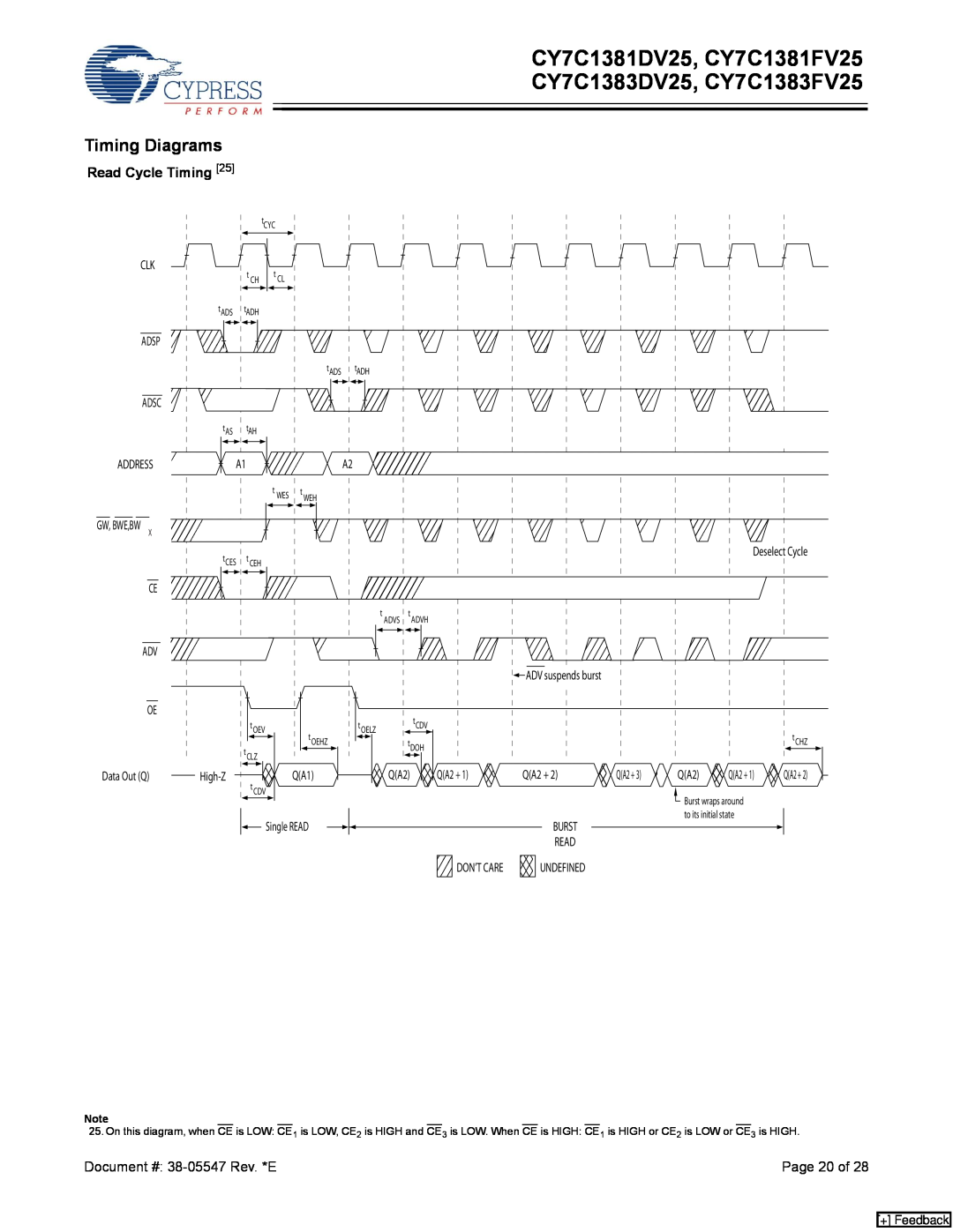
Timing Diagrams
CY7C1381DV25, CY7C1381FV25 CY7C1383DV25, CY7C1383FV25
Read Cycle Timing
+ Feedback
Timing Diagrams continued
CY7C1381DV25, CY7C1381FV25 CY7C1383DV25, CY7C1383FV25
+ Feedback
Data in D
Timing Diagrams continued
CY7C1381DV25, CY7C1381FV25 CY7C1383DV25, CY7C1383FV25
Read/Write Cycle Timing 25, 27
Page 22 of
Timing Diagrams continued
CY7C1381DV25, CY7C1381FV25 CY7C1383DV25, CY7C1383FV25
ZZ Mode Timing 29
Page 23 of
Ordering Information
CY7C1381DV25, CY7C1381FV25 CY7C1383DV25, CY7C1383FV25
Package Diagrams
CY7C1381DV25, CY7C1381FV25 CY7C1383DV25, CY7C1383FV25
Figure 1. 100-Pin Thin Plastic Quad Flat pack 14 x 20 x 1.4 mm
+ Feedback
Package Diagrams continued
CY7C1381DV25, CY7C1381FV25 CY7C1383DV25, CY7C1383FV25
Figure 2. 119-Ball BGA 14 x 22 x 2.4 mm
+ Feedback
Package Diagrams continued
CY7C1381DV25, CY7C1381FV25 CY7C1383DV25, CY7C1383FV25
Figure 3. 165-Ball FBGA 13 x 15 x 1.4 mm
165 FBGA 13 x 15 x 1.40 MM BB165D/BW165D
Document History Page
Issue Date
CY7C1381DV25, CY7C1381FV25 CY7C1383DV25, CY7C1383FV25
Flow-Through SRAM Document Number