CY7C68013A specifications
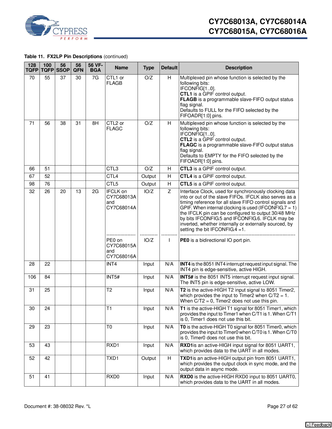
The Cypress CY7C68013A is a high-performance USB microcontroller that belongs to Cypress's FX2LP family, specifically designed for USB applications. This microcontroller is well-regarded for its versatility, making it a popular choice for developers engaged in USB-enabled projects.One of the main features of the CY7C68013A is its ability to support USB 2.0, with both high-speed (480 Mbps) and full-speed (12 Mbps) operation. This capability allows developers to take full advantage of the USB interface for data transfer, making it suitable for applications that require fast and efficient data communication. The device integrates a USB controller along with an 8051-compatible microcontroller, providing a seamless interface for USB transactions while also allowing for custom processing tasks.
The CY7C68013A offers 32 KB of internal RAM, which is a valuable resource for data buffering and temporary storage during data transfer operations. Additionally, it includes a programmable 8-bit I/O interface, which can be tailored to various application needs, facilitating control over peripheral devices. The microcontroller also features a 16-bit address bus and a 16-bit data bus, enhancing its ability to interface with external memory and components.
In terms of development, moving from concept to production becomes easier due to the availability of development kits and software support. The CY7C68013A is compatible with Cypress's EZ-USB development environment, which includes APIs and libraries that simplify the coding process. This software support empowers developers to create sophisticated USB-related applications without needing extensive background knowledge in USB protocol intricacies.
Regarding power efficiency, the CY7C68013A operates at low power consumption levels, making it suitable for battery-operated devices. It supports various low-power modes, which further enhances its appeal for portable applications.
Overall, the Cypress CY7C68013A stands out for its robust features, flexibility, and ease of use, making it an ideal choice for engineers working on USB-centric designs. Its combination of high-speed USB functionality, ample internal resources, and strong software support positions it as a go-to microcontroller for a wide variety of applications, ranging from consumer electronics to industrial systems.

