659,�$18$
General Notice
Precautions
About This Manual
Revision Status
Table of Contents
Maintenance
Product Description
Overview
General Characteristics
„ Holds 10 transparency films
Raster Graphics Mode
General Description
Printing
Printing Speed
Paper Feeding
Paper Specification
„ No curled, wrinkled, scuffing or torn paper be used
Paper Left Right Top Bottom
Printable Area
Width Length Margin Typ Min
Adjust Lever Settings
Setting Position of Adjust Lever
Paper Lever position Adjustment Value
Envelope
Environmental Conditions
Environmental Condition
Black Ink Cartridge
Ink Cartridge
Color Ink Cartridge
Electric Specification
Safety Approvals
Input Data Buffer
Reliability
Printer Language and Emulation
CE Marking
14.1 ESC/P Control Codes
„ Dot size control ESC e „ Raster header ESC D „ Raster body
Connector pin assignment and signals
Parallel Interface
Parallel InterfaceForward channel
Parallel I/F
Pin Signal Return In/Out Function Description Name GND pin
Parallel InterfaceReverse channel
Connect pin assignment and signals
Xflag Out
Parallel I/F Mode Typical time of tack
10. Typical Time of Tack
12. Connector pin assignment and signals
Serial Interface
11. Serial interface
13. X-ON/X-OFF, DTR protocol
Pin Signal Name Out Function Description
14. Connector pin assignment and signals
USBUniversal Serial Bus Interface
Interface selection
Prevention of data transfer time-out on Host
Ieee 1284.4 protocol
Bi-directional Command
Switches
Function
Control Code
Special Setting Mode
18. Special setting mode
LED Indications
17. Status printing
Errors
Indicators
19. Printer Status displayed on the control panel
Ink Out Paper Out Priority Black Color
„ When you need to perform test print after the repair
Initialization
Initialization Setting
Physical Specification
20. Consumables
Consumables and options
Classification Name
Operating Principles
Printer Mechanism
Printer Mechanism
Epson Stylus Photo Revision a
1 C257 PSB Power Supply Circuit
Operating Principles of Electric Circuit
Output Voltage
Voltage Usage
TRANST1
2 C259 Main Control Circuit
Major Elements
Major Elements
Location Function
Reset Circuit
Reset Circuit
Sensor Circuit
Sensor Circuit
Eeprom Control Circuit
Timer Circuit
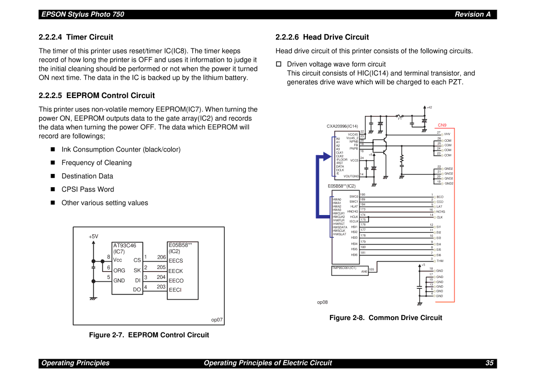
Head Drive Circuit
Paper Feed Pump Motor PF/Pump Motor Drive Circuit
Paper Feed Pump Motor Drive Circuit
Carriage MotorCR Motor Drive Circuit
10. Carriage Motor Drive Circuit
Troubleshooting
Check Point Signal Level Switch Mode
Sensor Check Point
Motor, Coil Resistance
Motor Location Check Point Resistance
LED Indication Condition Remedy
Error Indication
Paper Ink End Check Black Color
Symptoms and Corresponding Flow Chart
Unit Level Troubleshooting
Symptom Cause Flow Chart
E c k t h e Error S s a g e . R e f e r t o T a b le 3
A R T
Repair of the Power Supply Board
Unit Repair Power Supply Board
Sympto Condition Cause Check point Solution
Repair of the Control Board
Repair of the Control Board
Epson Stylus Photo Revision a
Symptom Condition Cause Check Point Solution
Unit Repair Printer Mechanism
10. Repair of the Printer Mechanism
11. Repair of the Printer Mechanism
12. Repair of the Printing Mechanism
13. Repair of the Printing Mechanism
14. Repair of the Printer Mechanism
15. Repair of the Printer Mechanism
Disassembly and Assembly
Tools
Precautions
Name Supplier Parts No Phillips Screw Driver
Check List
Work Completion Check
Classifi Check Point Status Cation
Disassembly
Flowchart below shows step-by step disassembly procedures
Housing Removal
Housing Removal
Circuit Boards Removal
Shield Plate, M/B Removal
E P O
Control Panel Removal
Control Panel Removal
Absorber Tray, AssemblyA Removal
Absorber Tray, AssemblyA Removal
Printer Mechanism Removal
Print Head Removal
E „ Be sure that the grounding plate is installed to
Print Head Installation
Pump, Assembly/Cap, Assembly Removal
„ Be careful not to damage the rubber part of the cap
11. Ink Tube
Motor, Assembly, CR Removal
Bi-D adjustment. See Bi-D Adjustment on
Motor Assembly PF Removal
15. Motor, Assembly, PF Installation
5.5 ASF, Assembly Removal
Paper Feed Roller Assembly Removal
E „ When removing or installing the Hopper
Roller Assembly, LD Left/Right Removal
18. Roller Assembly, LD Removal
Carriage Assembly Removal
19. Bush Parallel Adjust Removal
20. Carriage Assembly Removal
PE Sensor Assembly Removal
21. PE Sensor Assembly Removal
Roller, Assembly, PF Removal
23. Roller, Assembly, Paper Exit Removal
24. Roller, Assembly, PF Removal
HP Sensor Removal
25. HP Sensor Removal
Cartridge SensorSensor, I/C Removal
26. Bush Holder, Sensor, I/C Removal
29. Sensor, I/C Removal
Adjustment
Required Adjustment
Required Adjustment
Paper Gap Adjustment
Adjustment
„ Do not scratch special coated surface of the PF
Epson Stylus Photo Revision B
Adjustment by Adjustment Program
Adjustment Program
How to use the Adjustment Program
„ You have to go through the menu to input
Options in the Program and Keys to Use
Setting Destination Information
Head Voltage ID Adjustment
Head Angular Adjustment
Screw position for fixing the print head
Magnetized condition when the printer has been left
Adjustment, the following screen will be appeared
U Preventing from the CR motor fall into the non
Alone more then 5 minutes in the Head Anguler
Bi-D Adjustment
Bi-D Adjustment Pattern Sample
Head Cleaning
Initial Ink Charge
Counter Value for Ink Absorber
Protect Counter Reset
Protect Counter Value
Maintenance
Service Maintenance
Cleaning
„ Never use chemical solvents, such as thinner, to
Lubrication
„ Never use oil and the grease other than those
Lubrication Point
Type Name Epson Code Supplier
ASF
A R , 2 3
V e r a p p l y t h e o i l
Appendix
Connector Summary
Connector Summary for C259Main
Connector CN4
Major Component Unit
Connector CN5
Connector CN6
Connector CN7
Connector CN8
Connector CN10
10. Connector CN11
Component Layout
C259 Main Component Layout
Appendix Component Layout 101
Exploded Diagram
Exploded Diagram-1
Exploded Diagram for Epson Stylus Photo 750 2/3
Exploded Diagram for Epson Stylus Photo 750 3/3
Electric Circuit
Page
Page