4.6 Read/write Circuit
(4) Viterbi detection circuit
The sample hold waveform output from the adaptive equalizer circuit is sent to the Viterbi detection circuit. The Viterbi detection circuit demodulates data according to the survivor path sequence.
(5) Data separator circuit
The data separator circuit generates clocks in synchronization with the output of the adaptive equalizer circuit. To write data, the VFO circuit generates clocks in synchronization with the clock signals from a synthesizer.
(6) 8/9 GCR decoder
This circuit converts the
4.6.4 Time base generator circuit
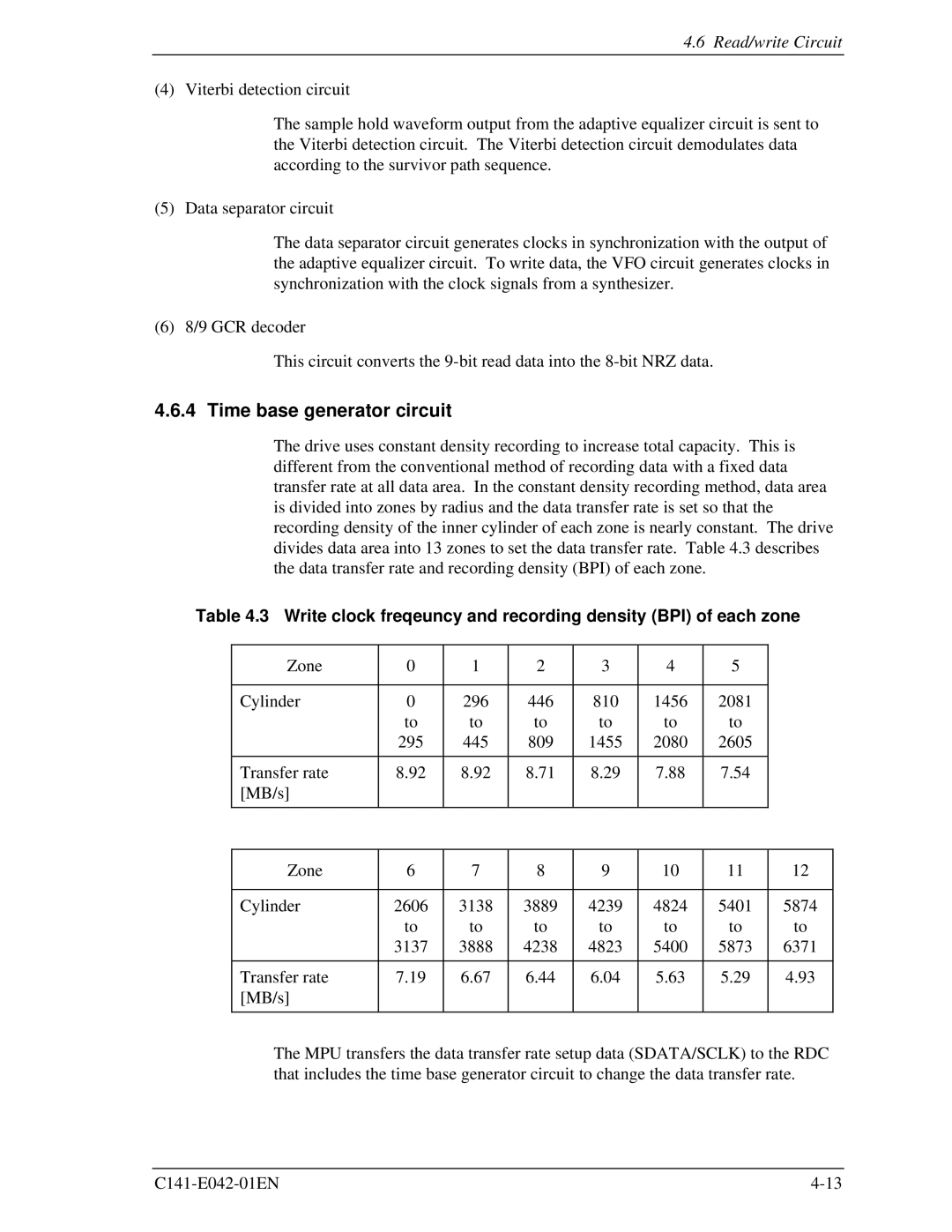
The drive uses constant density recording to increase total capacity. This is different from the conventional method of recording data with a fixed data transfer rate at all data area. In the constant density recording method, data area is divided into zones by radius and the data transfer rate is set so that the recording density of the inner cylinder of each zone is nearly constant. The drive divides data area into 13 zones to set the data transfer rate. Table 4.3 describes the data transfer rate and recording density (BPI) of each zone.
Table 4.3 Write clock freqeuncy and recording density (BPI) of each zone
Zone | 0 | 1 | 2 | 3 | 4 | 5 |
|
|
|
|
|
|
|
|
|
Cylinder | 0 | 296 | 446 | 810 | 1456 | 2081 |
|
| to | to | to | to | to | to |
|
| 295 | 445 | 809 | 1455 | 2080 | 2605 |
|
|
|
|
|
|
|
|
|
Transfer rate | 8.92 | 8.92 | 8.71 | 8.29 | 7.88 | 7.54 |
|
[MB/s] |
|
|
|
|
|
|
|
|
|
|
|
|
|
|
|
|
|
|
|
|
|
|
|
Zone | 6 | 7 | 8 | 9 | 10 | 11 | 12 |
|
|
|
|
|
|
|
|
Cylinder | 2606 | 3138 | 3889 | 4239 | 4824 | 5401 | 5874 |
| to | to | to | to | to | to | to |
| 3137 | 3888 | 4238 | 4823 | 5400 | 5873 | 6371 |
|
|
|
|
|
|
|
|
Transfer rate | 7.19 | 6.67 | 6.44 | 6.04 | 5.63 | 5.29 | 4.93 |
[MB/s] |
|
|
|
|
|
|
|
|
|
|
|
|
|
|
|
The MPU transfers the data transfer rate setup data (SDATA/SCLK) to the RDC that includes the time base generator circuit to change the data transfer rate.