EM78P259N/260N
Elan Microelectronics Corporation
Contents
Reset and Wake-up
TCC/WDT and Prescaler
Analog-To-Digital Converter ADC
6.1
11.1
11.2
11.3
11.4
Doc. Version Revision Description
Date
Features
General Description
Bit Microprocessor with OTP ROM
Block Diagram
Pin Assignment
Pin DIP/SOP
Pin DIP/SOP/SSOP
Symbol Pin No Type Function
Pin Description
EM78P259NP/M
EM78P260NP/M/KM
Function Description
Operational Registers
1 R0 Indirect Address Register
2 R1 Time Clock /Counter
EM78P259N/260N
Bit Microprocessor with OTP ROM Data Memory Configuration
Cont
5 R4 RAM Select Register
Bit 4 T
Bit
Bits 5~0
Bit 7 ~ Bit 4 C3 ~ C0 Calibrator of internal RC mode
6 R5 ~ R6 Port 5 ~ Port
7 R7 Port
Bit 7 ~ Bit
8 R8 Aisr ADC Input Select Register
9 R9 Adcon ADC Control Register
Bit 3 Adpd
RA Adoc ADC Offset Calibration Register
RB Addata Converted Value of ADC
Bit 5 ~ Bit 3 VOF2 ~ VOF0 Offset voltage bits
Bit 2 ~ Bit 0 Unimplemented, read as ‘0’
RC ADDATA1H Converted Value of ADC
RD ADDATA1L Converted Value of ADC
RE Interrupt Status 2 & Wake-up Control Register
RF Interrupt Status 2 Register
16 R10 ~ R3F
All of these are 8-bit general-purpose registers
Special Purpose Registers
Accumulator
Control Register
3 IOC50 ~ IOC70 I/O Port Control Register
4 IOC80 Comparator and Tcca Control Register
Bit 7 & Bit 6 Not used
Bit 4 & Bit 3 COS1 & COS0 Comparator/OP Select bits
Bit 6 Tccben Tccb enable bit 0 = disable Tccb
Bit 4 Tccbte Tccb signal edge
Tccc signal source
Bit 0 Tcccte Tccc signal edge
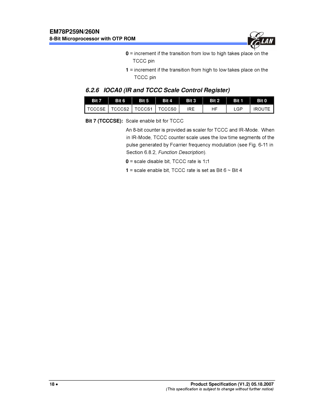
IOCA0 IR and Tccc Scale Control Register
Bit 3 IRE
Bit 2 HF
Bit 1 LGP
Bit 0 Iroute
IOCB0 Pull-down Control Register
IOCC0 Open-Drain Control Register
Bit PD57 PD56 PD55 PD54 PD53 PD52 PD51 PD50
Bit OD67 OD66 OD65 OD64 OD63 OD62 OD61 OD60
IOCD0 Pull-high Control Register
IOCE0 WDT Control & Interrupt Mask Registers
Bit PH57 PH56 PH55 PH54 PH53 PH52 PH51 PH50
Lpwtif interrupt enable bit
= Disable Lpwtif interrupt
= Enable Lpwtif interrupt
IOCF0 Interrupt Mask Register
12 IOC51 Tcca Counter
13 IOC61 Tccb Counter
14 IOC71 TCCBH/MSB Counter
15 IOC81 Tccc Counter
16 IOC91 Low Time Register
IOCA1 High Time Register
IOCB1 High/Low Time Scale Control Register
IOCC1 TCC Prescaler Counter
Bit 2 ~ Bit 0 LTS2 ~ LTS0 Low time scale bits
TCC prescaler counter can be read and written to
TCC/WDT and Prescaler
I/O Ports
MUX
I/O Port and I/O Control Register Circuit for P60 /INT
I/O Port and I/O Control Register Circuit for Port 50 ~ P57
Reset and Wake-up
Reset and Wake-up Operation
Usage of Port 5 Input Change Wake-up/Interrupt Function
Wake-up Wake-up and Interrupt
EM78P259N/260N
Select Segment
Signal Sleep Mode Normal Mode
Comparator
Address Name Reset Type Bit
Following summarizes the initialized values for registers
Name Reset Type Bit
HTR7 HTR6 HTR5 HTR4 HTR3 HTR2 HTR1 HTR0
Aisr
Controller Reset Block Diagram
Tcif
Interrupt
T and P Status under Status R3 Register
Event
EM78P259N/260N
Reti
Interrupt Vector Interrupt Status Priority
Analog-to-Digital Converter ADC
ADC Control Register AISR/R8, ADCON/R9, ADOC/RA
1.1 R8 Aisr ADC Input Select Register
Bit 7 ~ Bit 3 ADE3 Bit 2 ADE2
1.2 R9 Adcon AD Control Register
P54/TCC/VREF Pin Priority High Medium Low
P54
While the CPU is operating
= ADC is operating
RA Adoc AD Offset Calibration Register
ADC Operation during Sleep Mode
ADC Data Register ADDATA/RB, ADDATA1H/RC, ADDATA1L/RD
ADC Sampling Time
AD Conversion Time
Programming Process/Considerations
Programming Process
Follow these steps to obtain data from the ADC
Sample Demo Programs Define a General Register
Define a Control Register
ADC Control Register
Define Bits in Adcon
AD power on
Infrared Remote Control Application/PWM Waveform Generation
Overview
Function Description
Fcarrier
IRE Irout
Programming the Related Registers
IR/PWM Related Status/Data Registers
Address Name Bit
EM78P259N/260N
Timer/Counter
Under Tcca Counter IOC51
Under Tccb Counter IOC61
Under Tccc Counter IOC81
Comparator
Related Tccx Status/Data Registers
External Reference Signal
Comparator Output
Using a Comparator as an Operation Amplifier
Wake-up from Sleep Mode
Comparator Interrupt
Oscillator
Oscillator Modes
Oscillator Modes
Conditions
Crystal Oscillator/Ceramic Resonators Crystal
Oscillator Type
Frequency C1pF C2pF
External RC Oscillator Mode
18 Serial Mode Crystal/Resonator Circuit Diagram
Internal RC Oscillator Mode
Internal Drift Rate RC Frequency Temperature
Cext Rext Average Fosc 5V, 25C Average Fosc 3V, 25C
40C ~ +85C 3V~5.5V Total
Power-on Considerations
External Power-on Reset Circuit
Programmable WDT Time-out Period
Residual Voltage Protection
Vdd
EM78P259N
EM78P260N
Code Option
Code Option Register Word
Word Word1 Bit12 ~ Bit0
Word Bit Bit 6 Bit 5 Bit 4 Bit 3 Bit 2 Bit 1 Bit
= Pulses equal to 8/fc s is regarded as signal
= Pulses equal to 32/fc s is regarded as signal default
Bit Microprocessor with OTP ROM Bit 3 HLP
Bit 2 ~ 0 PR2 ~ PR0 Protect Bits
Bit 1 & Bit 0 RCM1, RCM0 RC mode selection bits
Instruction Set
Customer ID Register Word
Following are the EM78P259N/260N instruction set
Instruction Binary
Mnemonic Operation Status Affected
Absolute Maximum Ratings
Items Rating
DC Electrical Characteristics
Symbol Parameter Condition Min Typ Max Unit
Ta=25 C, VDD=5.0V±5%, VSS=0V
Internal RC Drift Rate
Voltage Min Typ Max
AD Converter Characteristics
Vdd=2.5V to 5.5V, Vss=0V, Ta=25C
Comparator OP Characteristics
Device Characteristics
Vdd = 5.0V, Vss=0V, Ta=25C
AC Electrical Characteristic
Symbol Parameter Conditions Min Typ Max Unit
Ta=25C, VDD=5V±5%, VSS=0V
Timing Diagrams
Reset Timing CLK=0
AC Test Input/Output Waveform
TCC Input Timing CLKS=0
Package Type
Package Information
18-Lead Plastic Dual in line Pdip 300 mil
Package Type Pin Count Package Size
18-Lead Plastic Small Outline SOP 300 mil
838
Lead Plastic Shrink Small Outline Ssop 209 mil
650
Lead Plastic Dual-in-line Pdip 300 mil
Lead Plastic Small Outline SOP 300 mil
Quality Assurance and Reliability
Address Trap Detect
Test Category Test Conditions Remarks