|
| Intel® 31244 |
|
| Intel® 31244 |
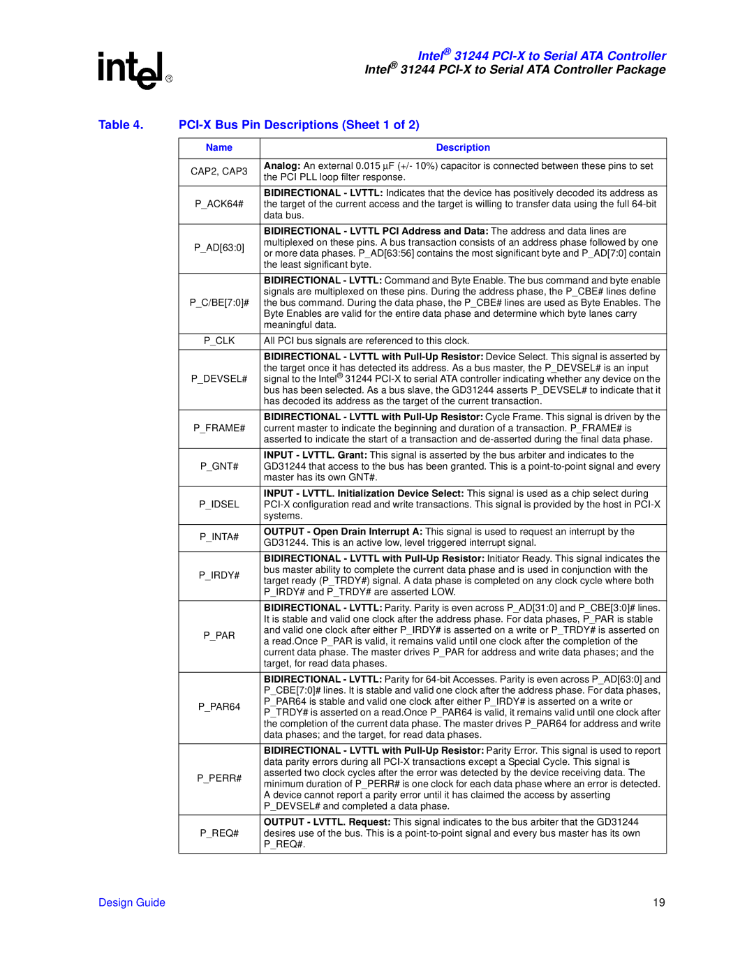
Table 4. |
| |
|
|
|
| Name | Description |
|
|
|
| CAP2, CAP3 | Analog: An external 0.015 ∝F (+/- 10%) capacitor is connected between these pins to set |
| the PCI PLL loop filter response. | |
|
| |
|
|
|
|
| BIDIRECTIONAL - LVTTL: Indicates that the device has positively decoded its address as |
| P_ACK64# | the target of the current access and the target is willing to transfer data using the full |
|
| data bus. |
|
|
|
|
| BIDIRECTIONAL - LVTTL PCI Address and Data: The address and data lines are |
| P_AD[63:0] | multiplexed on these pins. A bus transaction consists of an address phase followed by one |
| or more data phases. P_AD[63:56] contains the most significant byte and P_AD[7:0] contain | |
|
| |
|
| the least significant byte. |
|
|
|
|
| BIDIRECTIONAL - LVTTL: Command and Byte Enable. The bus command and byte enable |
|
| signals are multiplexed on these pins. During the address phase, the P_CBE# lines define |
| P_C/BE[7:0]# | the bus command. During the data phase, the P_CBE# lines are used as Byte Enables. The |
|
| Byte Enables are valid for the entire data phase and determine which byte lanes carry |
|
| meaningful data. |
|
|
|
| P_CLK | All PCI bus signals are referenced to this clock. |
|
|
|
|
| BIDIRECTIONAL - LVTTL with |
|
| the target once it has detected its address. As a bus master, the P_DEVSEL# is an input |
| P_DEVSEL# | signal to the Intel® 31244 |
|
| bus has been selected. As a bus slave, the GD31244 asserts P_DEVSEL# to indicate that it |
|
| has decoded its address as the target of the current transaction. |
|
|
|
|
| BIDIRECTIONAL - LVTTL with |
| P_FRAME# | current master to indicate the beginning and duration of a transaction. P_FRAME# is |
|
| asserted to indicate the start of a transaction and |
|
|
|
|
| INPUT - LVTTL. Grant: This signal is asserted by the bus arbiter and indicates to the |
| P_GNT# | GD31244 that access to the bus has been granted. This is a |
|
| master has its own GNT#. |
|
|
|
|
| INPUT - LVTTL. Initialization Device Select: This signal is used as a chip select during |
| P_IDSEL | |
|
| systems. |
|
|
|
| P_INTA# | OUTPUT - Open Drain Interrupt A: This signal is used to request an interrupt by the |
| GD31244. This is an active low, level triggered interrupt signal. | |
|
| |
|
|
|
|
| BIDIRECTIONAL - LVTTL with |
| P_IRDY# | bus master ability to complete the current data phase and is used in conjunction with the |
| target ready (P_TRDY#) signal. A data phase is completed on any clock cycle where both | |
|
| |
|
| P_IRDY# and P_TRDY# are asserted LOW. |
|
|
|
|
| BIDIRECTIONAL - LVTTL: Parity. Parity is even across P_AD[31:0] and P_CBE[3:0]# lines. |
|
| It is stable and valid one clock after the address phase. For data phases, P_PAR is stable |
| P_PAR | and valid one clock after either P_IRDY# is asserted on a write or P_TRDY# is asserted on |
| a read.Once P_PAR is valid, it remains valid until one clock after the completion of the | |
|
| |
|
| current data phase. The master drives P_PAR for address and write data phases; and the |
|
| target, for read data phases. |
|
|
|
|
| BIDIRECTIONAL - LVTTL: Parity for |
|
| P_CBE[7:0]# lines. It is stable and valid one clock after the address phase. For data phases, |
| P_PAR64 | P_PAR64 is stable and valid one clock after either P_IRDY# is asserted on a write or |
| P_TRDY# is asserted on a read.Once P_PAR64 is valid, it remains valid until one clock after | |
|
| |
|
| the completion of the current data phase. The master drives P_PAR64 for address and write |
|
| data phases; and the target, for read data phases. |
|
|
|
|
| BIDIRECTIONAL - LVTTL with |
|
| data parity errors during all |
| P_PERR# | asserted two clock cycles after the error was detected by the device receiving data. The |
| minimum duration of P_PERR# is one clock for each data phase where an error is detected. | |
|
| |
|
| A device cannot report a parity error until it has claimed the access by asserting |
|
| P_DEVSEL# and completed a data phase. |
|
|
|
|
| OUTPUT - LVTTL. Request: This signal indicates to the bus arbiter that the GD31244 |
| P_REQ# | desires use of the bus. This is a |
|
| P_REQ#. |
|
|
|
Design Guide | 19 |
