4.5Trace Impedance
All signal layers require controlled impedance of 50 Ω +/- 15%, microstrip or stripline where appropriate, unless otherwise specified. Selecting the appropriate board
All recommendations described in this document assume a Twid 5 mil 50 Ω signal trace, unless otherwise specified. When a different stack up is used the trace widths must be adjusted appropriately. When wider traces are used, the trace spacing must be adjusted accordingly (linearly).
It is highly recommended that a 2D Field Solver be used to design the
http://emclab.umr.edu/pcbtlc/
http://www.westak.com/techcenter/imped/
The following website link provides a useful basic guideline for calculating trace parameters:
http://www.ultracad.com/calc.htm
Note: Using stripline transmission lines may give better results than microstrip. This is due to the difficulty of precisely controlling the dielectric constant of the solder mask, and the difficulty in limiting the plated thickness of microstrip conductors, which may substantially increase
4.5.1Differential Impedance
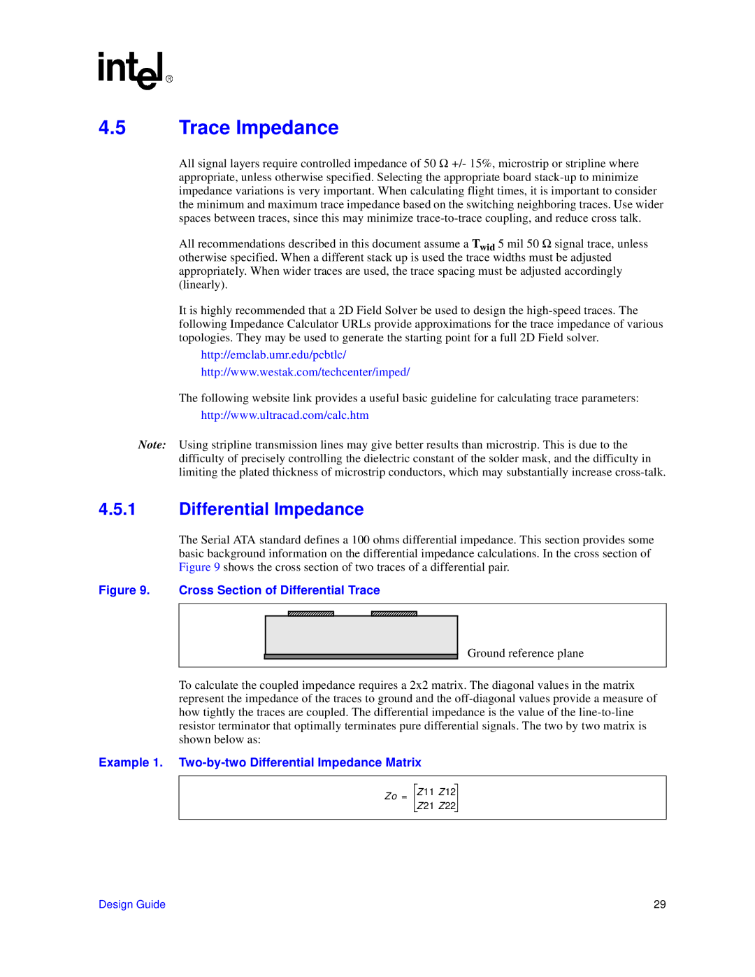
The Serial ATA standard defines a 100 ohms differential impedance. This section provides some basic background information on the differential impedance calculations. In the cross section of Figure 9 shows the cross section of two traces of a differential pair.
Figure 9. Cross Section of Differential Trace
Ground reference plane
To calculate the coupled impedance requires a 2x2 matrix. The diagonal values in the matrix represent the impedance of the traces to ground and the
Example 1. Two-by-two Differential Impedance Matrix
Zo =
Z11 Z12 Z21 Z22
Design Guide | 29 |