Intel® 31244 PCI-X to Serial ATA Controller
About This Document
Table 2. | Terminology and Definition (Sheet 2 of 3) |
|
|
|
|
| |||||||
|
|
|
|
|
|
|
|
|
|
|
|
|
|
| Term |
|
|
|
|
|
|
| Definition | ||||
|
|
|
|
|
|
|
|
|
|
|
|
|
|
|
|
|
|
|
|
|
|
|
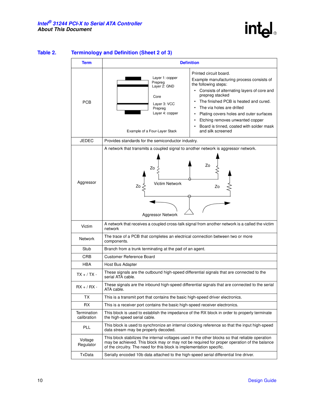
| Printed circuit board. | |||
|
|
|
|
|
|
| Layer 1: copper |
| Example manufacturing process consists of | ||||
|
|
|
|
|
|
|
| ||||||
|
|
|
|
|
|
| Prepreg |
| the following steps: | ||||
|
|
|
|
|
|
| Layer 2: GND |
| |||||
|
|
|
|
|
|
|
| • Consists of alternating layers of core and | |||||
|
|
|
|
|
|
|
|
|
| ||||
|
|
|
|
|
|
| Core |
| prepreg stacked | ||||
|
|
|
|
|
|
|
|
|
|
|
| ||
| PCB |
|
|
|
|
| Layer 3: VCC |
| • The finished PCB is heated and cured. | ||||
|
|
|
|
|
|
|
| • The via holes are drilled | |||||
|
|
|
|
|
|
| Prepreg |
| |||||
|
|
|
|
|
|
| Layer 4: copper |
| • Plating covers holes and outer surfaces | ||||
|
|
|
|
|
|
|
| ||||||
|
|
|
|
|
|
|
|
|
| • Etching removes unwanted copper | |||
|
|
|
|
|
|
|
|
|
| • Board is tinned, coated with solder mask | |||
|
|
|
| Example of a |
| and silk screened | |||||||
|
|
|
|
|
|
|
|
|
|
|
|
| |
| JEDEC | Provides standards for the semiconductor industry. | |||||||||||
|
|
|
|
|
|
|
|
|
|
|
|
| |
|
| A network that transmits a coupled signal to another network is aggressor network. | |||||||||||
| Aggressor |
|
|
|
|
| Zo |
|
| Zo |
|
|
|
|
|
|
|
|
|
|
|
|
| ||||
|
|
|
|
|
|
|
|
|
|
|
| ||
|
|
|
|
|
|
|
|
|
|
|
|
| |
|
|
|
|
|
|
|
|
|
|
|
|
| |
|
|
|
|
|
|
|
|
|
|
|
|
| |
|
|
|
| Zo | Victim Network | ||||||||
|
|
|
|
|
|
| Zo | ||||||
|
|
|
|
|
|
|
|
|
|
|
|
|
|
|
|
|
|
|
|
|
|
|
|
|
|
|
|
| Aggressor Network | |
|
| |
Victim | A network that receives a coupled | |
network | ||
| ||
|
| |
Network | The trace of a PCB that completes an electrical connection between two or more | |
components. | ||
| ||
|
| |
Stub | Branch from a trunk terminating at the pad of an agent. | |
|
| |
CRB | Customer Reference Board | |
|
| |
HBA | Host Bus Adapter | |
|
| |
TX + / TX - | These signals are the outbound | |
serial ATA cable. | ||
| ||
|
| |
RX + / RX - | These signals are the inbound | |
ATA cable. | ||
| ||
|
| |
TX | This is a transmit port that contains the basic | |
|
| |
RX | This is a receiver port contains the basic | |
|
| |
Termination | This block is used to establish the impedance of the RX block in order to properly terminate | |
calibration | the | |
|
| |
PLL | This block is used to synchronize an internal clocking reference so that the input | |
data stream may be properly decoded. | ||
| ||
|
| |
Voltage | This block stabilizes the internal voltages used in the other blocks so that reliable operation | |
may be achieved. This block may or may not be required for proper operation of the balance | ||
Regulator | ||
of the circuitry. The need for this block is implementation specific. | ||
| ||
|
| |
TxData | Serially encoded 10b data attached to the |
10 | Design Guide |
