Intel® 31244 PCI-X to Serial ATA Controller
Routing Guidelines
4.2Crosstalk
Crosstalk is caused by capacitive and inductive coupling between signals. Crosstalk is composed of both backward and forward crosstalk components. Backward crosstalk creates an induced signal on victim network that propagates in the opposite direction of the aggressor signal. Forward crosstalk creates a signal that propagates in the same direction as the aggressor signal.
Circuit board analysis software is used to analyze your board layout for crosstalk problems. Examples of 2D analysis tools include Parasitic Parameters from ANSOFT* and XFS from Quad Design*. Crosstalk problems occur when circuit etch lines run in parallel. When board analysis software is not available, the layout maintains minimum spacing between parallel circuit signals lines.
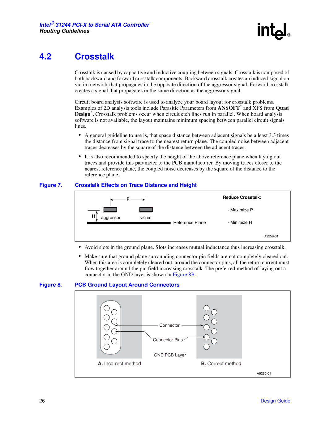
•A general guideline to use is, that space distance between adjacent signals be a least 3.3 times the distance from signal trace to the nearest return plane. The coupled noise between adjacent traces decreases by the square of the distance between the adjacent traces.
•It is also recommended to specify the height of the above reference plane when laying out traces and provide this parameter to the PCB manufacturer. By moving traces closer to the nearest reference plane, the coupled noise decreases by the square of the distance to the reference plane.
Figure 7. Crosstalk Effects on Trace Distance and Height
H
|
|
|
| P |
|
| Reduce Crosstalk: | |
|
|
|
|
|
| |||
|
|
|
|
|
| |||
|
|
|
|
|
|
|
| - Maximize P |
|
|
|
|
|
|
|
| |
|
|
|
|
|
|
|
| |
|
|
|
|
|
|
|
|
|
aggressor |
| victim | - Minimize H | |||||
|
|
|
|
|
|
| Reference Plane | |
•Avoid slots in the ground plane. Slots increases mutual inductance thus increasing crosstalk.
•Make sure that ground plane surrounding connector pin fields are not completely cleared out. When this area is completely cleared out, around the connector pins, all the return current must flow together around the pin field increasing crosstalk. The preferred method of laying out a connector in the GND layer is shown in Figure 8B.
Figure 8. PCB Ground Layout Around Connectors
Connector
Connector Pins ![]()
![]()
GND PCB Layer
A. Incorrect method | B. Correct method |
26 | Design Guide |