Terminations: | 11 |
This chapter provides the requirements for
The
1.Embedded or motherboard application (non PCI/X
2.
When the application is a PCI/X
The GD31244 uses 10 K
•Rmin = [Vcc(max) - Vol’]/[Iol+(16 x Iol)] where 16 is the maximum number of loads
•Rmax = [Vcc(min) - Vx]/[num_loads x Imin] where Vx = 0.7 VCC for 3.3 V signaling:
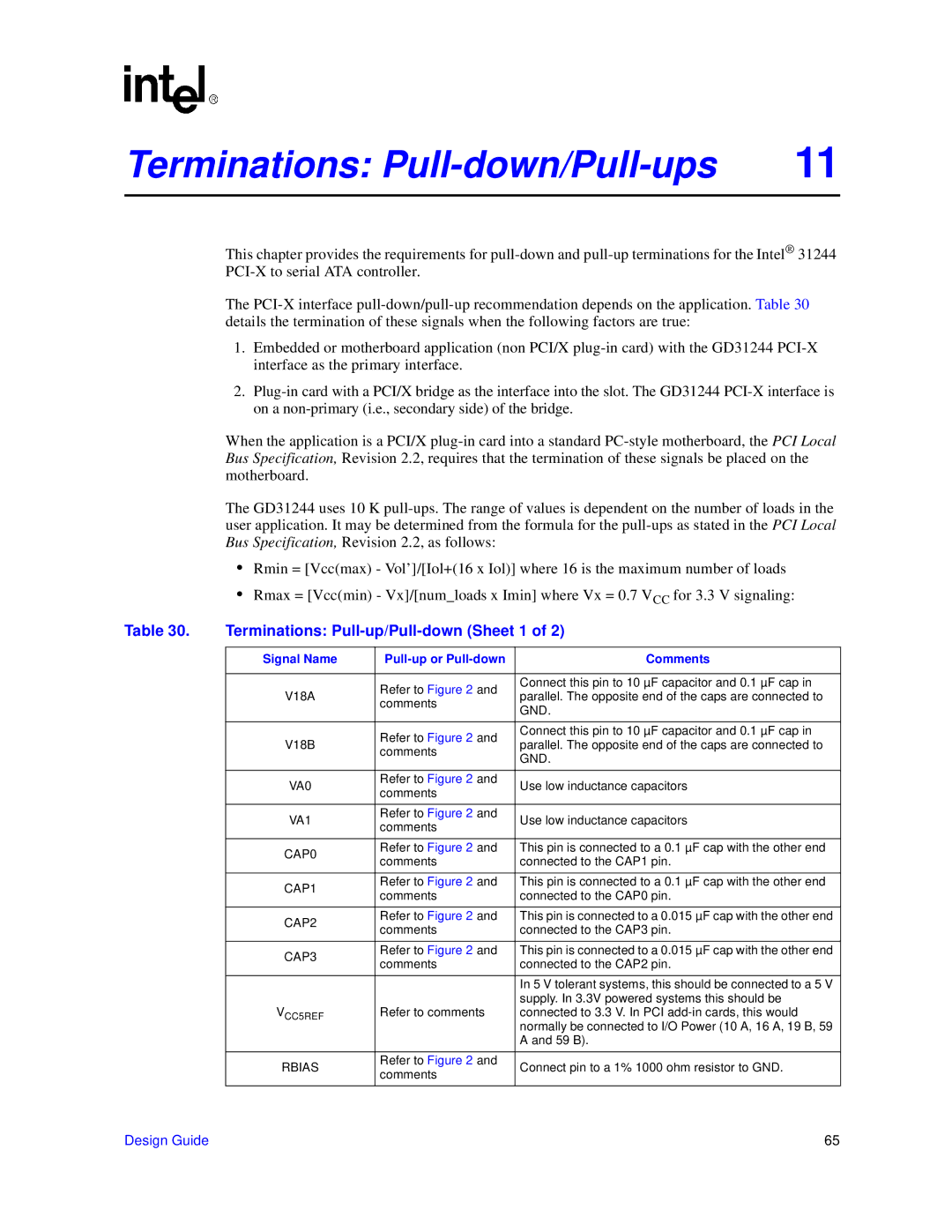
Table 30. | Terminations: | ||
|
|
|
|
| Signal Name |
| Comments |
|
|
|
|
|
| Refer to Figure 2 and | Connect this pin to 10 µF capacitor and 0.1 µF cap in |
| V18A | parallel. The opposite end of the caps are connected to | |
| comments | ||
|
| GND. | |
|
|
| |
|
|
|
|
|
| Refer to Figure 2 and | Connect this pin to 10 µF capacitor and 0.1 µF cap in |
| V18B | parallel. The opposite end of the caps are connected to | |
| comments | ||
|
| GND. | |
|
|
| |
|
|
|
|
| VA0 | Refer to Figure 2 and | Use low inductance capacitors |
| comments | ||
|
|
| |
|
|
|
|
| VA1 | Refer to Figure 2 and | Use low inductance capacitors |
| comments | ||
|
|
| |
|
|
|
|
| CAP0 | Refer to Figure 2 and | This pin is connected to a 0.1 µF cap with the other end |
| comments | connected to the CAP1 pin. | |
|
| ||
|
|
|
|
| CAP1 | Refer to Figure 2 and | This pin is connected to a 0.1 µF cap with the other end |
| comments | connected to the CAP0 pin. | |
|
| ||
|
|
|
|
| CAP2 | Refer to Figure 2 and | This pin is connected to a 0.015 µF cap with the other end |
| comments | connected to the CAP3 pin. | |
|
| ||
|
|
|
|
| CAP3 | Refer to Figure 2 and | This pin is connected to a 0.015 µF cap with the other end |
| comments | connected to the CAP2 pin. | |
|
| ||
|
|
|
|
|
|
| In 5 V tolerant systems, this should be connected to a 5 V |
| VCC5REF |
| supply. In 3.3V powered systems this should be |
| Refer to comments | connected to 3.3 V. In PCI | |
|
|
| normally be connected to I/O Power (10 A, 16 A, 19 B, 59 |
|
|
| A and 59 B). |
|
|
|
|
| RBIAS | Refer to Figure 2 and | Connect pin to a 1% 1000 ohm resistor to GND. |
| comments | ||
|
|
| |
|
|
|
|
Design Guide | 65 |
