Intel® 31244 PCI-X to Serial ATA Controller
Printed Circuit Board (PCB) Methodology
6.1.1Intel® 31244 PCI-X to Serial ATA Controller HBA Stackup
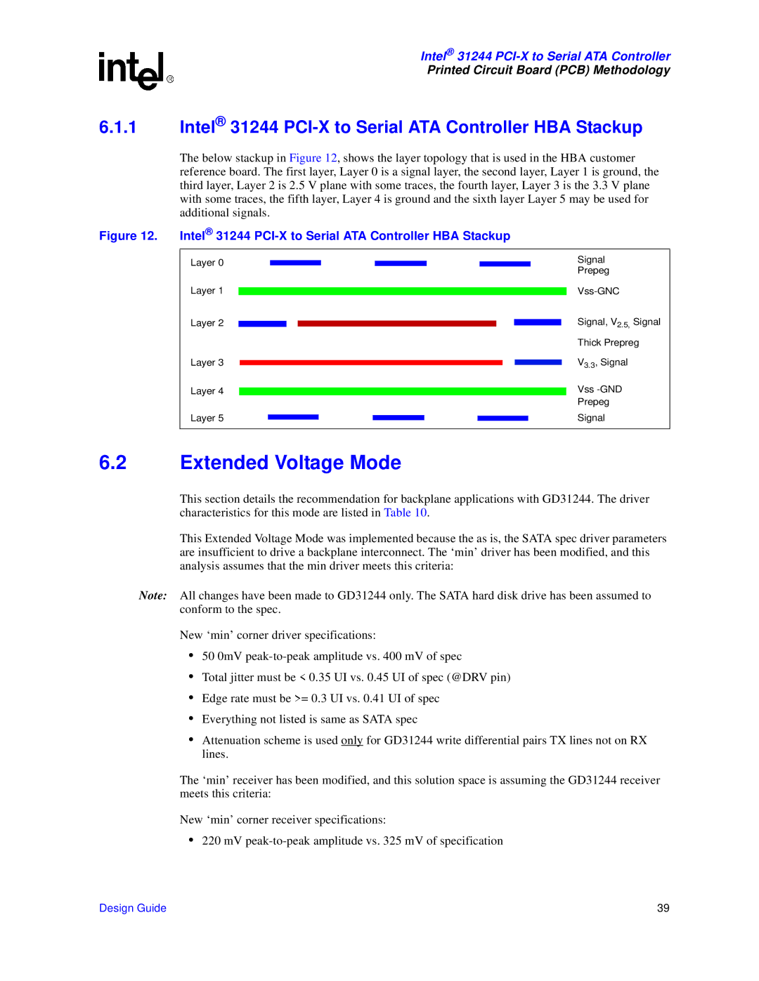
The below stackup in Figure 12, shows the layer topology that is used in the HBA customer reference board. The first layer, Layer 0 is a signal layer, the second layer, Layer 1 is ground, the third layer, Layer 2 is 2.5 V plane with some traces, the fourth layer, Layer 3 is the 3.3 V plane with some traces, the fifth layer, Layer 4 is ground and the sixth layer Layer 5 may be used for additional signals.
Figure 12. Intel® 31244 PCI-X to Serial ATA Controller HBA Stackup
Layer 0
Layer 1
Layer 2
Layer 3
Layer 4
Layer 5
Signal
Prepeg
Signal, V2.5, Signal
Thick Prepreg
V3.3, Signal
Vss
Prepeg
Signal
6.2Extended Voltage Mode
This section details the recommendation for backplane applications with GD31244. The driver characteristics for this mode are listed in Table 10.
This Extended Voltage Mode was implemented because the as is, the SATA spec driver parameters are insufficient to drive a backplane interconnect. The ‘min’ driver has been modified, and this analysis assumes that the min driver meets this criteria:
Note: All changes have been made to GD31244 only. The SATA hard disk drive has been assumed to conform to the spec.
New ‘min’ corner driver specifications:
•50 0mV
•Total jitter must be < 0.35 UI vs. 0.45 UI of spec (@DRV pin)
•Edge rate must be >= 0.3 UI vs. 0.41 UI of spec
•Everything not listed is same as SATA spec
•Attenuation scheme is used only for GD31244 write differential pairs TX lines not on RX lines.
The ‘min’ receiver has been modified, and this solution space is assuming the GD31244 receiver meets this criteria:
New ‘min’ corner receiver specifications:
•220 mV
Design Guide | 39 |
