Intel® 31244 PCI-X to Serial ATA Controller
Routing Guidelines
Routing Guidelines | 4 |
This chapter provides routing guidelines for layout and design of a printed circuit board using the GD31244. The
• | power distribution | • | decoupling |
• | minimizing crosstalk | • | layout considerations when routing the SATA bus |
4.1General Routing Guidelines
This section details general routing guidelines for connecting the GD31244. The order in which signals are routed varies from designer to designer. Some designers prefer to route all clock signals first, while others prefer to route all
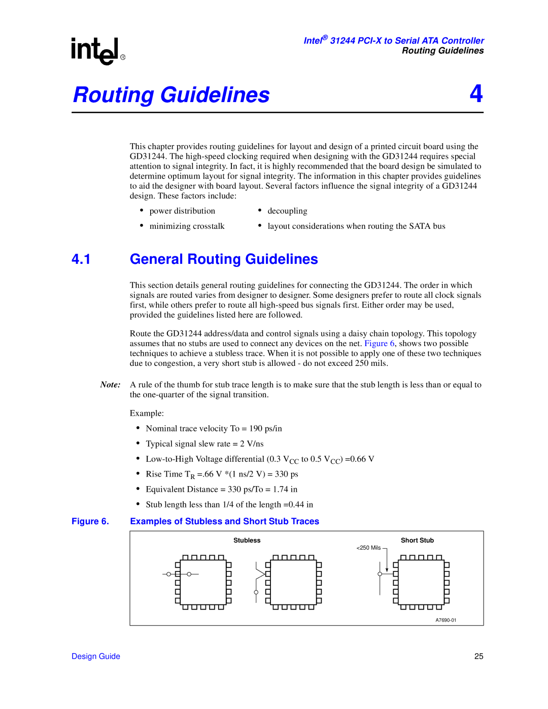
Route the GD31244 address/data and control signals using a daisy chain topology. This topology assumes that no stubs are used to connect any devices on the net. Figure 6, shows two possible techniques to achieve a stubless trace. When it is not possible to apply one of these two techniques due to congestion, a very short stub is allowed - do not exceed 250 mils.
Note: A rule of the thumb for stub trace length is to make sure that the stub length is less than or equal to the
Example:
•Nominal trace velocity To = 190 ps/in
•Typical signal slew rate = 2 V/ns
•
•Rise Time TR =.66 V *(1 ns/2 V) = 330 ps
•Equivalent Distance = 330 ps/To = 1.74 in
•Stub length less than 1/4 of the length =0.44 in
Figure 6. Examples of Stubless and Short Stub Traces
Stubless | Short Stub |
<250 Mils
Design Guide | 25 |