Intel® 31244 PCI-X to Serial ATA Controller
Intel® 31244
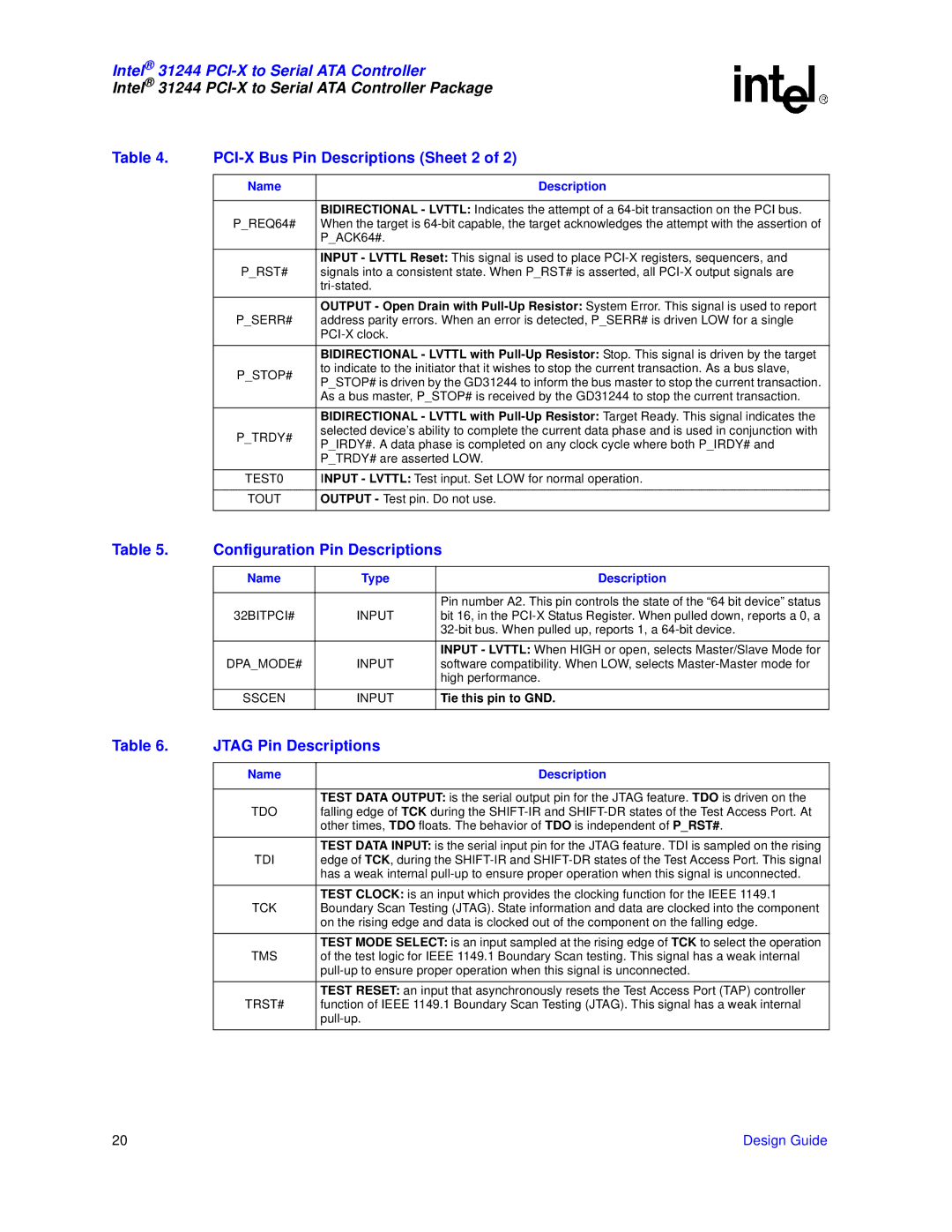
Table 4. |
| |
|
|
|
| Name | Description |
|
|
|
|
| BIDIRECTIONAL - LVTTL: Indicates the attempt of a |
| P_REQ64# | When the target is |
|
| P_ACK64#. |
|
|
|
|
| INPUT - LVTTL Reset: This signal is used to place |
| P_RST# | signals into a consistent state. When P_RST# is asserted, all |
|
| |
|
|
|
|
| OUTPUT - Open Drain with |
| P_SERR# | address parity errors. When an error is detected, P_SERR# is driven LOW for a single |
|
| |
|
|
|
|
| BIDIRECTIONAL - LVTTL with |
| P_STOP# | to indicate to the initiator that it wishes to stop the current transaction. As a bus slave, |
| P_STOP# is driven by the GD31244 to inform the bus master to stop the current transaction. | |
|
| |
|
| As a bus master, P_STOP# is received by the GD31244 to stop the current transaction. |
|
|
|
|
| BIDIRECTIONAL - LVTTL with |
| P_TRDY# | selected device’s ability to complete the current data phase and is used in conjunction with |
| P_IRDY#. A data phase is completed on any clock cycle where both P_IRDY# and | |
|
| |
|
| P_TRDY# are asserted LOW. |
|
|
|
| TEST0 | INPUT - LVTTL: Test input. Set LOW for normal operation. |
|
|
|
| TOUT | OUTPUT - Test pin. Do not use. |
|
|
|
Table 5. | Configuration Pin Descriptions | ||
|
|
|
|
| Name | Type | Description |
|
|
|
|
|
|
| Pin number A2. This pin controls the state of the “64 bit device” status |
| 32BITPCI# | INPUT | bit 16, in the |
|
|
| |
|
|
|
|
|
|
| INPUT - LVTTL: When HIGH or open, selects Master/Slave Mode for |
| DPA_MODE# | INPUT | software compatibility. When LOW, selects |
|
|
| high performance. |
|
|
|
|
| SSCEN | INPUT | Tie this pin to GND. |
|
|
|
|
Table 6. | JTAG Pin Descriptions | |
|
|
|
| Name | Description |
|
|
|
|
| TEST DATA OUTPUT: is the serial output pin for the JTAG feature. TDO is driven on the |
| TDO | falling edge of TCK during the |
|
| other times, TDO floats. The behavior of TDO is independent of P_RST#. |
|
|
|
|
| TEST DATA INPUT: is the serial input pin for the JTAG feature. TDI is sampled on the rising |
| TDI | edge of TCK, during the |
|
| has a weak internal |
|
|
|
|
| TEST CLOCK: is an input which provides the clocking function for the IEEE 1149.1 |
| TCK | Boundary Scan Testing (JTAG). State information and data are clocked into the component |
|
| on the rising edge and data is clocked out of the component on the falling edge. |
|
|
|
|
| TEST MODE SELECT: is an input sampled at the rising edge of TCK to select the operation |
| TMS | of the test logic for IEEE 1149.1 Boundary Scan testing. This signal has a weak internal |
|
| |
|
|
|
|
| TEST RESET: an input that asynchronously resets the Test Access Port (TAP) controller |
| TRST# | function of IEEE 1149.1 Boundary Scan Testing (JTAG). This signal has a weak internal |
|
| |
|
|
|
20 | Design Guide |
