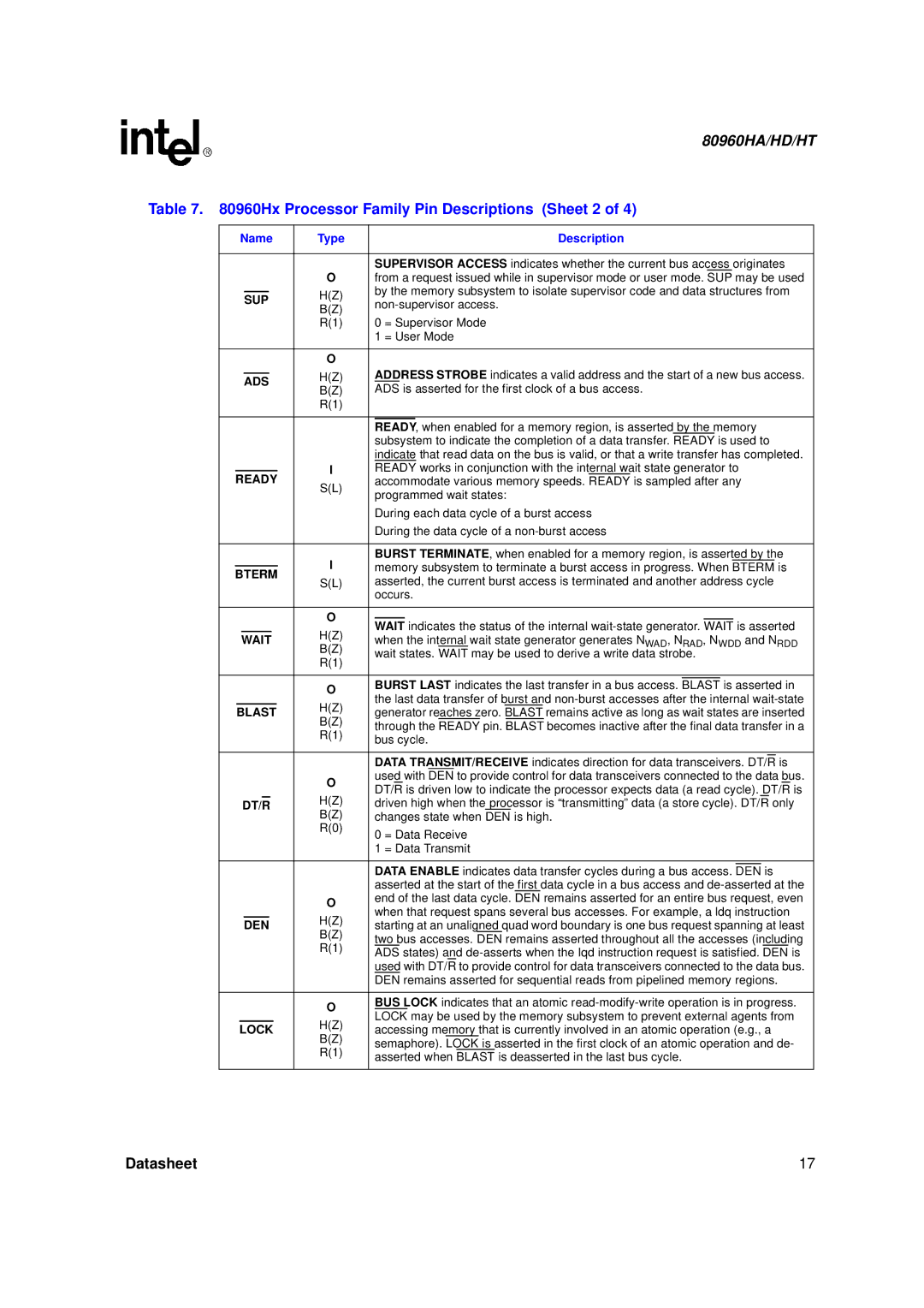
Intel 80960HA, 80960HD, 80960HT manual Hx Processor Family Pin Descriptions Sheet 2, Sup

Models: 80960HT 80960HA 80960HD

1 104
Download 104 pages 37.32 Kb
Page 17
Image 17

80960HA/HD/HT

Table 7. 80960Hx Processor Family Pin Descriptions (Sheet 2 of 4)


Name


Type


Description


O

SUPERVISOR ACCESS indicates whether the current bus access originates


from a request issued while in supervisor mode or user mode. SUP may be used


H(Z)

by the memory subsystem to isolate supervisor code and data structures from


SUP


non-supervisor access.


B(Z)


R(1)

0 = Supervisor Mode


1 = User Mode


O


H(Z)

ADDRESS STROBE indicates a valid address and the start of a new bus access.


ADS


B(Z)

ADS is asserted for the first clock of a bus access.


R(1)


READY, when enabled for a memory region, is asserted by the memory


subsystem to indicate the completion of a data transfer.

READY

is used to


indicate that read data on the bus is valid, or that a write transfer has completed.


I

READY works in conjunction with the internal wait state generator to


READY


S(L)

accommodate various memory speeds. READY is sampled after any


programmed wait states:


During each data cycle of a burst access


During the data cycle of a non-burst access


I

BURST TERMINATE, when enabled for a memory region, is asserted by the


memory subsystem to terminate a burst access in progress. When BTERM is

BTERM


S(L)

asserted, the current burst access is terminated and another address cycle


occurs.


O


WAIT indicates the status of the internal wait-state generator. WAIT is asserted


H(Z)


WAIT


when the internal wait state generator generates NWAD, NRAD, NWDD and NRDD


B(Z)


wait states. WAIT may be used to derive a write data strobe.


R(1)


BURST LAST indicates the last transfer in a bus access.


is asserted in


O

BLAST


the last data transfer of burst and non-burst accesses after the internal wait-state


H(Z)


BLAST


generator reaches zero. BLAST remains active as long as wait states are inserted


B(Z)


through the READY pin. BLAST becomes inactive after the final data transfer in a


R(1)


bus cycle.


is


DATA TRANSMIT/RECEIVE indicates direction for data transceivers. DT/R


O

used with DEN to provide control for data transceivers connected to the data bus.


DT/R is driven low to indicate the processor expects data (a read cycle). DT/R is


H(Z)


DT/R


driven high when the processor is “transmitting” data (a store cycle). DT/R only


B(Z)

changes state when DEN is high.


R(0)

0 = Data Receive


1 = Data Transmit


DATA ENABLE indicates data transfer cycles during a bus access.


is


DEN


asserted at the start of the first data cycle in a bus access and de-asserted at the


O

end of the last data cycle. DEN remains asserted for an entire bus request, even


when that request spans several bus accesses. For example, a ldq instruction


H(Z)


DEN


starting at an unaligned quad word boundary is one bus request spanning at least


B(Z)


two bus accesses. DEN remains asserted throughout all the accesses (including


R(1)


ADS states) and de-asserts when the Iqd instruction request is satisfied. DEN is


used with DT/R to provide control for data transceivers connected to the data bus.


DEN remains asserted for sequential reads from pipelined memory regions.


O

BUS LOCK indicates that an atomic read-modify-write operation is in progress.


LOCK may be used by the memory subsystem to prevent external agents from


H(Z)


LOCK


accessing memory that is currently involved in an atomic operation (e.g., a


B(Z)


semaphore). LOCK is asserted in the first clock of an atomic operation and de-


R(1)


asserted when BLAST is deasserted in the last bus cycle.


Datasheet

17

Page 17
Image 17
Intel 80960HA, 80960HD, 80960HT manual Hx Processor Family Pin Descriptions Sheet 2, Sup

80960HT, 80960HA, 80960HD specifications

The Intel 80960 family of microprocessors, introduced in the late 1980s, marked a significant evolution in the landscape of embedded systems and high-performance computing. The series included notable members such as the 80960HD, 80960HA, and 80960HT, each offering distinct features, technologies, and characteristics tailored for specific applications.

The Intel 80960HD was primarily designed for high-performance applications, such as real-time processing and advanced embedded control systems. With a robust architecture, the 80960HD featured a 32-bit data bus and a 32-bit address bus, enabling it to access a larger memory space and providing superior performance for computational tasks. It included a sophisticated instruction set that facilitated efficient execution, particularly for computationally intensive tasks. The internal architecture also supported pipelining, allowing multiple instructions to be processed simultaneously, thus enhancing throughput.

The 80960HA variant was tailored for high-availability applications, making it ideal for embedded systems where reliability is paramount. This model incorporated features that emphasized fault tolerance and stability, ensuring that systems relying on it could maintain operational integrity even in the event of component failures. The 80960HA showcased enhanced error detection and correction capabilities, which contributed to its reputation as a dependable choice for mission-critical applications.

On the other hand, the 80960HT was designed to meet the needs of high-performance telecommunications and networking applications. Recognized for its ability to handle multiple tasks concurrently, the 80960HT included advanced features such as built-in support for multitasking and real-time processing. This made it an excellent fit for applications that demanded rapid data handling and processing, such as routers and switches in networking environments. Its architecture allowed for efficient context switching, ensuring that multiple processes could execute seamlessly.

All three variants utilized the same family architecture, enabling easy integration and compatibility across different applications. They also supported various memory management techniques, such as virtual memory and caching, enhancing their performance in diverse operating conditions. With their combination of high processing power, reliability, and flexibility, the Intel 80960 family of microprocessors played a crucial role in advancing embedded computing technologies, paving the way for modern-day processors and systems. The 80960 series remains a noteworthy chapter in the evolution of microprocessor design, reflecting the growing demands of the computing landscape during its time.