μPD75P308
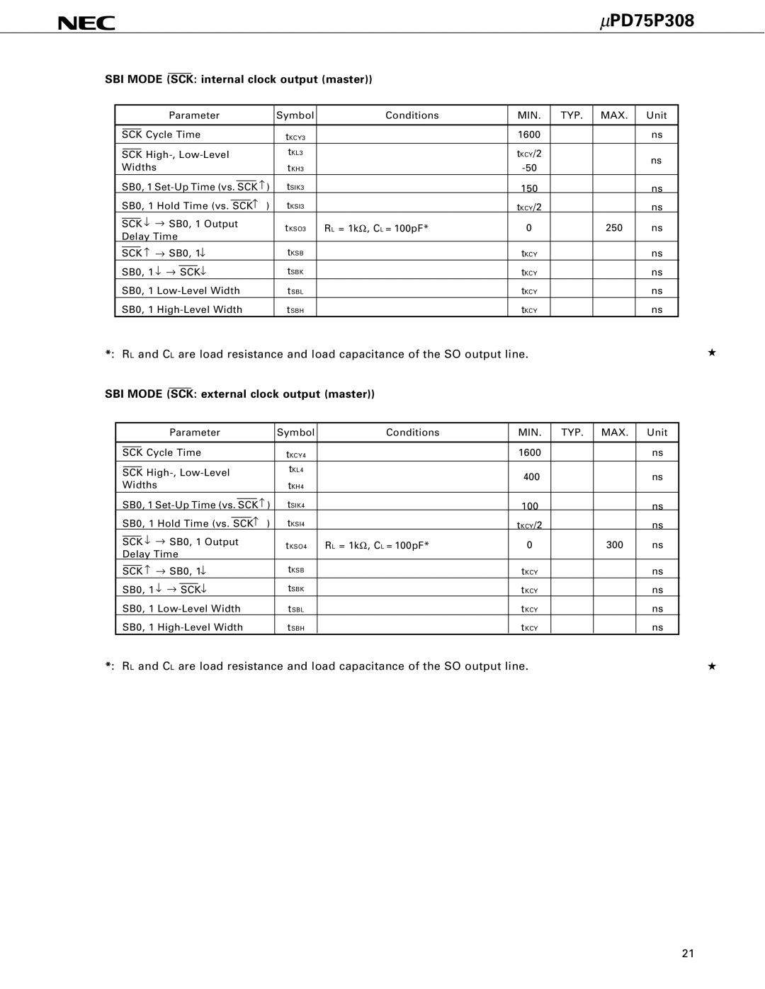
SBI MODE (SCK: internal clock output (master))
|
|
|
|
|
|
| Parameter | Symbol | Conditions | MIN. | TYP. | MAX. | Unit | ||||||
|
|
|
|
|
|
|
|
|
|
|
|
|
|
|
| ||||
|
|
|
|
|
|
|
|
|
| 1600 |
|
| ns | ||||||
|
| SCK | Cycle Time | tKCY3 |
|
|
| ||||||||||||
|
|
|
|
|
|
|
| tKL3 |
| tKCY/2 |
|
|
| ||||||
|
| SCK |
|
|
| ns | |||||||||||||
| Widths |
|
|
|
|
|
|
| tKH3 |
|
|
| |||||||
|
|
|
|
|
|
|
|
|
|
|
| ||||||||
| SB0, 1 |
| − ) | tSIK3 |
|
|
|
|
| ||||||||||
SCK |
| 150 |
|
| ns | ||||||||||||||
| SB0, 1 Hold Time (vs. |
|
| − ) | tKSI3 |
|
|
|
|
| |||||||||
SCK |
| tKCY/2 |
|
| ns | ||||||||||||||
|
| ↓ → SB0, 1 Output |
|
|
|
|
|
| |||||||||||
| SCK | tKSO3 | RL = 1kΩ, CL = 100pF* | 0 |
| 250 | ns | ||||||||||||
| Delay Time |
|
|
|
|
|
|
| |||||||||||
|
|
|
|
|
|
|
|
|
|
|
|
| |||||||
|
|
|
|
| − → |
|
| ↓ | tKSB |
|
|
|
|
| |||||
| SCK |
|
|
| tKCY |
|
| ns | |||||||||||
|
|
| SB0, 1 |
|
|
|
| ||||||||||||
| SB0, 1 | ↓ → |
| ↓ | tSBK |
| tKCY |
|
| ns | |||||||||
|
|
|
|
| |||||||||||||||
|
|
| SCK |
|
|
|
| ||||||||||||
| SB0, 1 | tSBL |
| tKCY |
|
| ns | ||||||||||||
| SB0, 1 | tSBH |
| tKCY |
|
| ns | ||||||||||||
*: RL and CL are load resistance and load capacitance of the SO output line.
SBI MODE (SCK: external clock output (master))
|
|
|
|
| Parameter | Symbol | Conditions | MIN. | TYP. | MAX. | Unit | ||||||
|
|
|
|
|
|
|
|
|
|
|
|
|
|
|
| ||
|
|
|
|
|
|
|
|
|
| 1600 |
|
| ns | ||||
| SCK | Cycle Time | tKCY4 |
|
|
| |||||||||||
|
|
|
|
|
|
|
|
|
|
|
| tKL4 |
|
|
|
|
|
| SCK |
| 400 |
|
| ns | |||||||||||
|
|
|
|
| |||||||||||||
| Widths |
|
|
|
|
|
|
| tKH4 |
|
|
| |||||
|
|
|
|
|
|
|
|
|
|
|
|
| |||||
| SB0, 1 |
| − ) | tSIK4 |
|
|
|
|
| ||||||||
| SCK |
| 100 |
|
| ns | |||||||||||
| SB0, 1 Hold Time (vs. |
|
| − ) | tKSI4 |
|
|
|
|
| |||||||
| SCK |
| tKCY/2 |
|
| ns | |||||||||||
|
| ↓ → SB0, 1 Output |
|
|
|
|
|
| |||||||||
| SCK | tKSO4 | RL = 1kΩ, CL = 100pF* | 0 |
| 300 | ns | ||||||||||
| Delay Time |
| |||||||||||||||
|
|
|
|
|
|
| |||||||||||
|
|
|
| − → |
|
| ↓ | tKSB |
|
|
|
|
| ||||
| SCK |
|
|
| tKCY |
|
| ns | |||||||||
|
| SB0, 1 |
|
|
|
| |||||||||||
| SB0, 1 ↓ → |
| ↓ | tSBK |
| tKCY |
|
| ns | ||||||||
| SCK |
|
|
| |||||||||||||
| SB0, 1 | tSBL |
| tKCY |
|
| ns | ||||||||||
| SB0, 1 | tSBH |
| tKCY |
|
| ns | ||||||||||
*: RL and CL are load resistance and load capacitance of the SO output line.
★
★
21