★
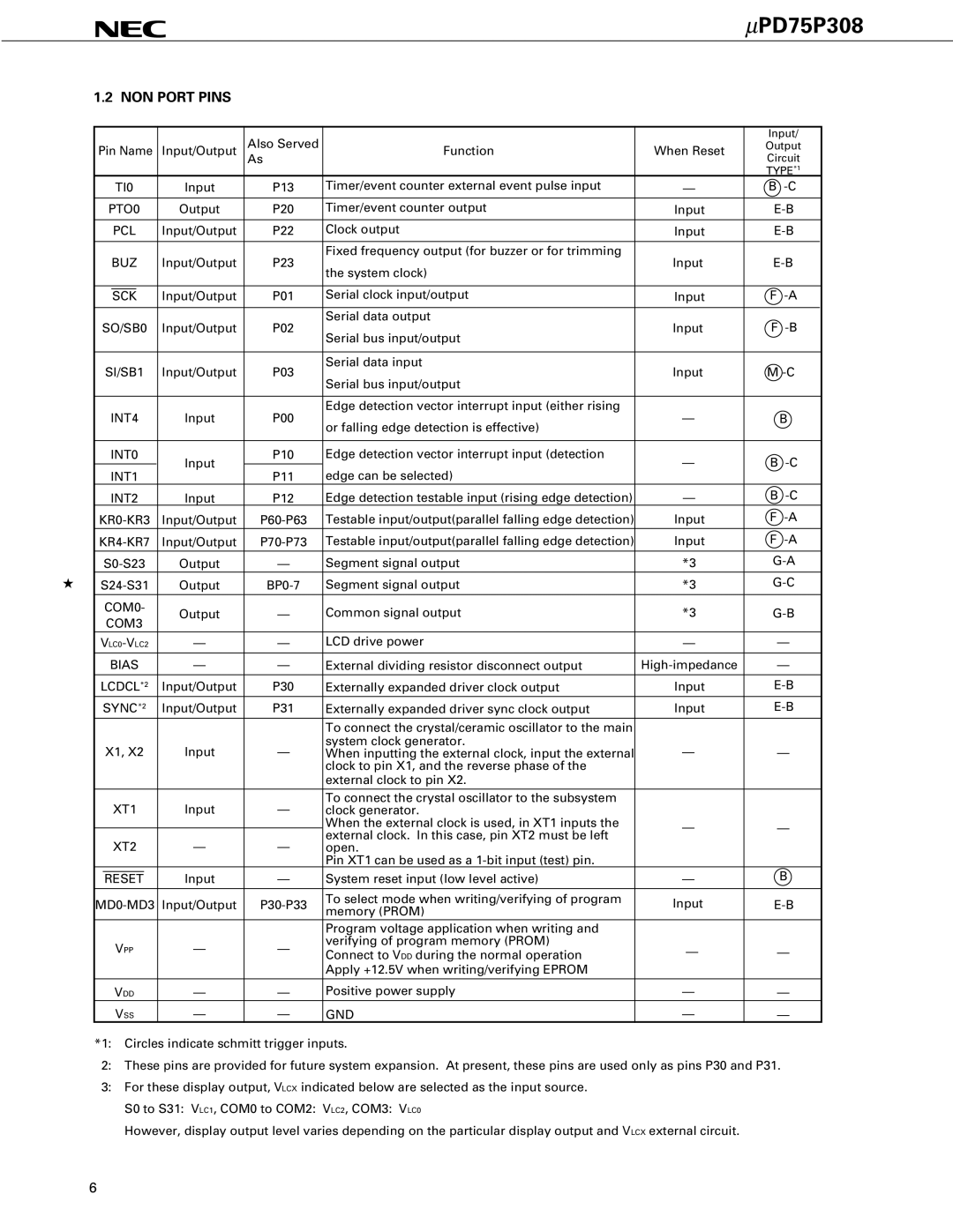
1.2 NON PORT PINS
|
|
|
|
|
| Also Served |
|
| Input/ | ||
Pin Name | Input/Output | Function | When Reset | Output | |||||||
|
|
|
|
|
| As |
|
| Circuit | ||
|
|
|
|
|
|
|
|
| TYPE*1 | ||
|
| TI0 | Input | P13 | Timer/event counter external event pulse input | — | B | ||||
|
|
|
|
|
|
|
|
|
| ||
| PTO0 | Output | P20 | Timer/event counter output | Input | ||||||
|
|
|
|
|
|
|
|
|
| ||
|
| PCL | Input/Output | P22 | Clock output | Input | |||||
|
|
|
|
|
|
|
|
|
|
| |
|
| BUZ | Input/Output | P23 | Fixed frequency output (for buzzer or for trimming | Input | |||||
|
| the system clock) | |||||||||
|
|
|
|
|
|
|
|
|
| ||
|
|
|
|
|
|
|
|
|
|
| |
|
|
|
| Input/Output | P01 | Serial clock input/output | Input | F | |||
|
| SCK |
|
| |||||||
|
|
|
|
|
|
|
|
|
|
| |
SO/SB0 | Input/Output | P02 | Serial data output | Input | F | ||||||
Serial bus input/output | |||||||||||
|
|
|
|
|
|
|
|
|
| ||
|
|
|
|
|
|
|
|
|
|
| |
| SI/SB1 | Input/Output | P03 | Serial data input | Input | M | |||||
| Serial bus input/output | ||||||||||
|
|
|
|
|
|
|
|
|
| ||
|
|
|
|
|
|
|
|
|
|
| |
| INT4 | Input | P00 | Edge detection vector interrupt input (either rising | — |
|
| ||||
| or falling edge detection is effective) |
|
| ||||||||
|
|
|
|
|
|
|
|
|
| ||
|
|
|
|
|
|
|
|
|
|
| |
| INT0 | Input | P10 | Edge detection vector interrupt input (detection | — | B | |||||
| INT1 | P11 | edge can be selected) | ||||||||
|
|
|
|
| |||||||
| INT2 | Input | P12 | Edge detection testable input (rising edge detection) | — | B | |||||
Input/Output | Testable input/output(parallel falling edge detection) | Input | F | ||||||||
| Input/Output | Testable input/output(parallel falling edge detection) | Input | F | |||||||
| Output | — | Segment signal output | *3 | |||||||
Output | Segment signal output | *3 | |||||||||
| COM0- | Output | — | Common signal output | *3 | ||||||
| COM3 | ||||||||||
|
|
|
|
|
|
| |||||
— | — | LCD drive power | — |
| — | ||||||
|
|
|
|
|
|
|
|
| |||
| BIAS | — | — | External dividing resistor disconnect output |
| — | |||||
LCDCL*2 | Input/Output | P30 | Externally expanded driver clock output | Input | |||||||
| SYNC*2 | Input/Output | P31 | Externally expanded driver sync clock output | Input | ||||||
|
|
|
|
|
|
| To connect the crystal/ceramic oscillator to the main |
|
|
| |
| X1, X2 | Input | — | system clock generator. | — |
| — | ||||
| When inputting the external clock, input the external |
| |||||||||
|
|
|
|
|
|
| clock to pin X1, and the reverse phase of the |
|
|
| |
|
|
|
|
|
|
| external clock to pin X2. |
|
|
| |
|
| XT1 | Input | — | To connect the crystal oscillator to the subsystem |
|
|
| |||
|
| clock generator. |
|
|
| ||||||
|
|
|
|
|
|
| When the external clock is used, in XT1 inputs the | — |
| — | |
|
| XT2 | — | — | external clock. In this case, pin XT2 must be left |
| |||||
|
|
|
|
| |||||||
|
| open. |
|
|
| ||||||
|
|
|
|
|
|
| Pin XT1 can be used as a |
|
|
| |
|
|
| Input | — | System reset input (low level active) | — |
| B | |||
| RESET |
| |||||||||
| Input/Output | To select mode when writing/verifying of program | Input | ||||||||
memory (PROM) | |||||||||||
|
|
|
|
|
|
|
|
|
| ||
|
|
|
|
|
|
| Program voltage application when writing and |
|
|
| |
|
| VPP | — | — | verifying of program memory (PROM) | — |
| — | |||
|
| Connect to VDD during the normal operation |
| ||||||||
|
|
|
|
|
|
| Apply +12.5V when writing/verifying EPROM |
|
|
| |
|
| VDD | — | — | Positive power supply | — |
| — | |||
|
| VSS | — | — | GND | — |
| — | |||
*1: Circles indicate schmitt trigger inputs.
2:These pins are provided for future system expansion. At present, these pins are used only as pins P30 and P31.
3:For these display output, VLCX indicated below are selected as the input source.
S0 to S31: VLC1, COM0 to COM2: VLC2, COM3: VLC0
However, display output level varies depending on the particular display output and VLCX external circuit.
6