μPD75P308
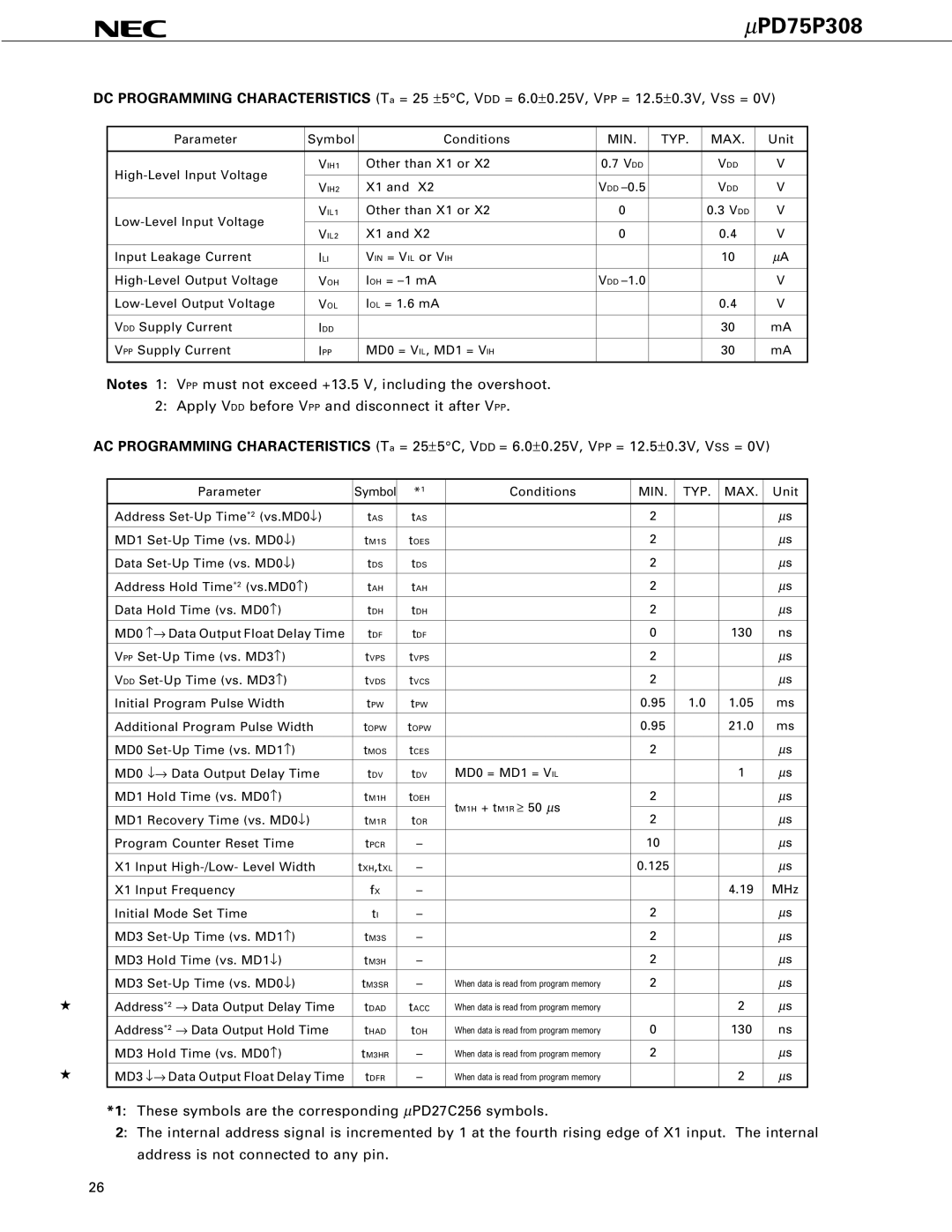
DC PROGRAMMING CHARACTERISTICS (Ta = 25 ±5°C, VDD = 6.0±0.25V, VPP = 12.5±0.3V, VSS = 0V)
Parameter | Symbol | Conditions | MIN. | TYP. | MAX. | Unit |
|
|
|
|
|
|
|
VIH1 | Other than X1 or X2 | 0.7 VDD |
| VDD | V | |
|
|
|
|
|
| |
VIH2 | X1 and X2 | VDD |
| VDD | V | |
|
| |||||
|
|
|
|
|
|
|
VIL1 | Other than X1 or X2 | 0 |
| 0.3 VDD | V | |
|
|
|
|
|
| |
VIL2 | X1 and X2 | 0 |
| 0.4 | V | |
|
| |||||
|
|
|
|
|
|
|
Input Leakage Current | ILI | VIN = VIL or VIH |
|
| 10 | μA |
|
|
|
|
|
|
|
VOH | IOH = | VDD |
|
| V | |
|
|
|
|
|
|
|
VOL | IOL = 1.6 mA |
|
| 0.4 | V | |
|
|
|
|
|
|
|
VDD Supply Current | IDD |
|
|
| 30 | mA |
|
|
|
|
|
|
|
VPP Supply Current | IPP | MD0 = VIL, MD1 = VIH |
|
| 30 | mA |
|
|
|
|
|
|
|
Notes 1: VPP must not exceed +13.5 V, including the overshoot.
2: Apply VDD before VPP and disconnect it after VPP.
AC PROGRAMMING CHARACTERISTICS (Ta = 25±5°C, VDD = 6.0±0.25V, VPP = 12.5±0.3V, VSS = 0V)
| Parameter | Symbol | *1 | Conditions | MIN. | TYP. | MAX. | Unit |
| Address | tAS | tAS |
| 2 |
|
| μs |
| MD1 | tM1S | tOES |
| 2 |
|
| μs |
|
|
|
|
|
|
|
|
|
| Data | tDS | tDS |
| 2 |
|
| μs |
|
|
|
|
|
|
|
|
|
| Address Hold Time*2 (vs.MD0−) | tAH | tAH |
| 2 |
|
| μs |
| Data Hold Time (vs. MD0−) | tDH | tDH |
| 2 |
|
| μs |
|
|
|
|
|
|
|
|
|
| MD0 −→ Data Output Float Delay Time | tDF | tDF |
| 0 |
| 130 | ns |
|
|
|
|
|
|
|
|
|
| VPP | tVPS | tVPS |
| 2 |
|
| μs |
|
|
|
|
|
|
|
|
|
| VDD | tVDS | tVCS |
| 2 |
|
| μs |
|
|
|
|
|
|
|
|
|
| Initial Program Pulse Width | tPW | tPW |
| 0.95 | 1.0 | 1.05 | ms |
|
|
|
|
|
|
|
|
|
| Additional Program Pulse Width | tOPW | tOPW |
| 0.95 |
| 21.0 | ms |
|
|
|
|
|
|
|
|
|
| MD0 | tMOS | tCES |
| 2 |
|
| μs |
|
|
|
|
|
|
|
|
|
| MD0 ↓→ Data Output Delay Time | tDV | tDV | MD0 = MD1 = VIL |
|
| 1 | μs |
|
|
|
|
|
|
|
|
|
| MD1 Hold Time (vs. MD0−) | tM1H | tOEH | tM1H + tM1R ≥ 50 μs | 2 |
|
| μs |
|
|
|
|
|
|
|
| |
| MD1 Recovery Time (vs. MD0↓) | tM1R | tOR | 2 |
|
| μs | |
|
|
|
| |||||
|
|
|
|
|
|
|
|
|
| Program Counter Reset Time | tPCR | – |
| 10 |
|
| μs |
|
|
|
|
|
|
|
|
|
| X1 Input | tXH,tXL | – |
| 0.125 |
|
| μs |
|
|
|
|
|
|
|
|
|
| X1 Input Frequency | fX | – |
|
|
| 4.19 | MHz |
|
|
|
|
|
|
|
|
|
| Initial Mode Set Time | tI | – |
| 2 |
|
| μs |
|
|
|
|
|
|
|
|
|
| MD3 | tM3S | – |
| 2 |
|
| μs |
|
|
|
|
|
|
|
|
|
| MD3 Hold Time (vs. MD1↓) | tM3H | – |
| 2 |
|
| μs |
|
|
|
|
|
|
|
|
|
| MD3 | tM3SR | – | When data is read from program memory | 2 |
|
| μs |
|
|
|
|
|
|
|
|
|
★ | Address*2 → Data Output Delay Time | tDAD | tACC | When data is read from program memory |
|
| 2 | μs |
| Address*2 → Data Output Hold Time | tHAD | tOH | When data is read from program memory | 0 |
| 130 | ns |
| MD3 Hold Time (vs. MD0−) | tM3HR | – | When data is read from program memory | 2 |
|
| μs |
★ |
|
|
|
|
|
|
|
|
MD3 ↓→ Data Output Float Delay Time | tDFR | – | When data is read from program memory |
|
| 2 | μs | |
|
|
|
|
|
|
|
|
|
*1: These symbols are the corresponding μPD27C256 symbols.
2: The internal address signal is incremented by 1 at the fourth rising edge of X1 input. The internal address is not connected to any pin.
26