μPD75P308
3.3 PROGRAM MEMORY READ PROCEDURE
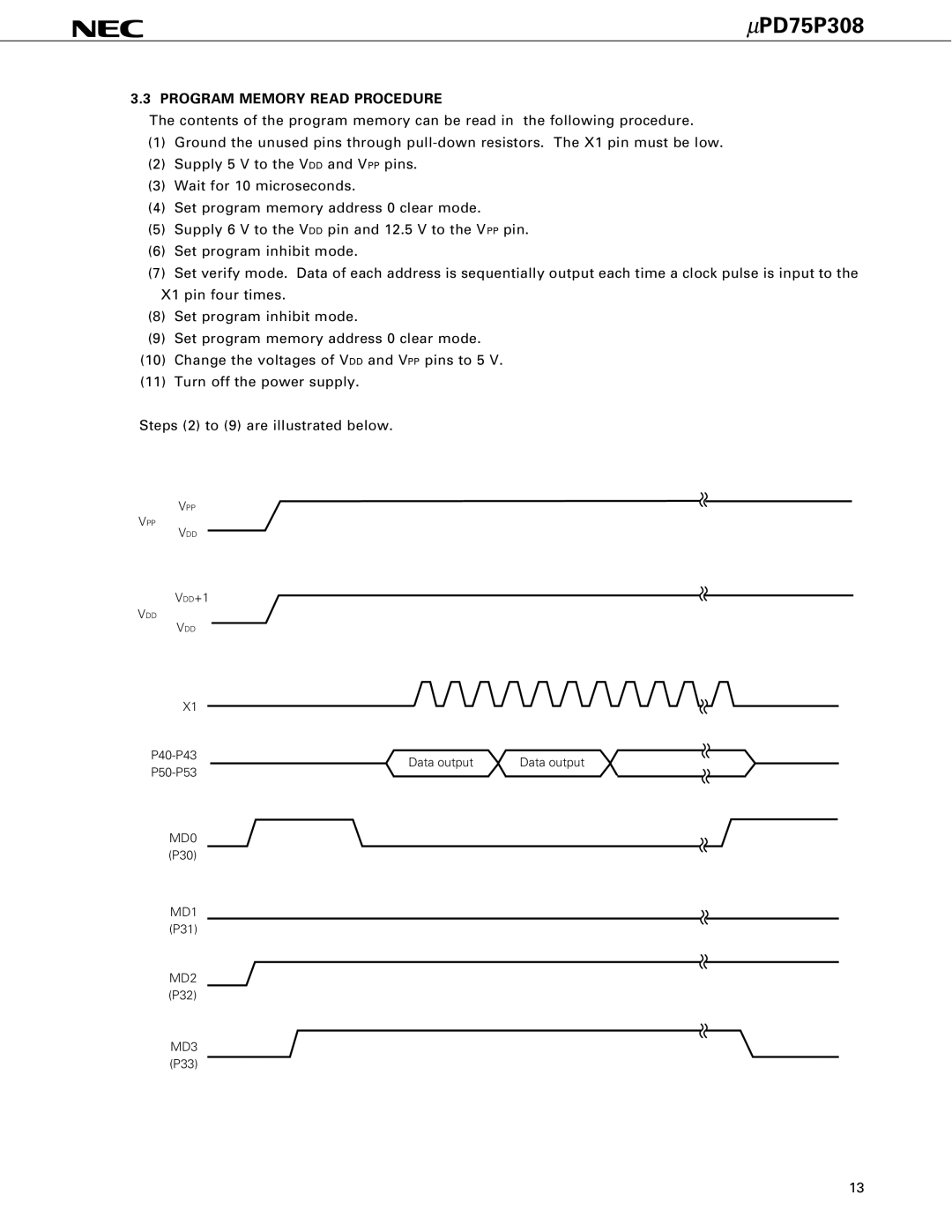
The contents of the program memory can be read in the following procedure.
(1)Ground the unused pins through
(2)Supply 5 V to the VDD and VPP pins.
(3)Wait for 10 microseconds.
(4)Set program memory address 0 clear mode.
(5)Supply 6 V to the VDD pin and 12.5 V to the VPP pin.
(6)Set program inhibit mode.
(7)Set verify mode. Data of each address is sequentially output each time a clock pulse is input to the X1 pin four times.
(8)Set program inhibit mode.
(9)Set program memory address 0 clear mode.
(10)Change the voltages of VDD and VPP pins to 5 V.
(11)Turn off the power supply.
Steps (2) to (9) are illustrated below.
VPP
VPP
VDD
VDD+1
VDD
VDD
X1 |
|
| |
Data output | Data output | ||
|
|
MD0
(P30)
MD1
(P31)
MD2
(P32)
MD3
(P33)
13