μPD75P308
1.3 PIN INPUT/OUTPUT CIRCUITS
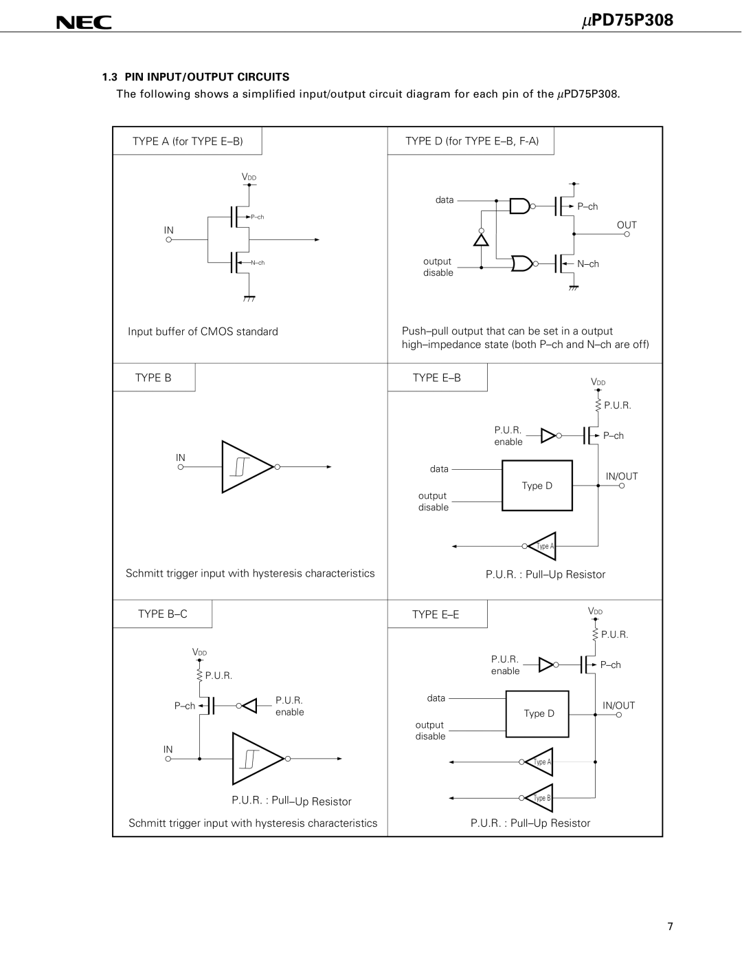
The following shows a simplified input/output circuit diagram for each pin of the μPD75P308.
TYPE A (for TYPE |
| TYPE D (for TYPE |
| |
VDD |
|
|
|
|
|
| data |
| |
|
|
|
| |
|
|
| OUT | |
IN |
|
|
| |
|
|
|
| |
| output |
| ||
|
| disable |
|
|
Input buffer of CMOS standard | ||||
|
| |||
TYPE B |
| TYPE |
| VDD |
|
|
|
| |
|
|
|
| P.U.R. |
|
|
| P.U.R. | |
|
|
| enable | |
|
|
|
| |
IN |
| data |
|
|
|
|
| IN/OUT | |
|
|
| Type D | |
|
| output |
| |
|
|
|
| |
|
| disable |
|
|
|
|
| Type A |
|
Schmitt trigger input with hysteresis characteristics |
| P.U.R. : | ||
TYPE |
| TYPE |
| VDD |
|
|
|
| P.U.R. |
VDD |
|
| P.U.R. |
|
|
|
| ||
P.U.R. |
|
| enable | |
|
|
| ||
|
|
|
| |
P.U.R. | data |
| IN/OUT | |
enable |
| Type D | ||
| output |
| ||
|
|
|
| |
|
| disable |
|
|
IN |
|
|
|
|
|
|
| Type A |
|
P.U.R. : |
| Type B |
| |
|
|
| ||
Schmitt trigger input with hysteresis characteristics |
| P.U.R. : | ||
7
