QUATECH, INC
MPAP-100 RS-232 PCMCIA SYNCHRONOUS ADAPTER
Users Manual
for PCMCIA Card Standard compatible machines
Synchronous Communications Adapter
WARRANTY INFORMATION
MPAP-100
PRODUCT DESCRIPTION Single Channel PCMCIA RS-232-D
Copyright 2001 Quatech, Inc
Table of Contents
5.2.1 Tying a configuration to a particular socket
5.3 OS/2 Client Driver Configuration Examples
5.4 Monitoring The Status Of PCMCIA Cards
22.1.4 Older Versions of Card and Socket Services
Table of Contents
10.3.1 Using channel A for both transmit and receive
Accessing the SCC while FIFOs are enabled
1.1 System Requirements
1 Introduction
2 Hardware Installation
3 DOS / Windows 3.x Software Installation
3.1 MPAP-100 Client Driver for DOS
3.1.1 DOS client driver installation
DEVICE=drive\path\MPAP1CL.SYS S#,B#,I#,C ... S#,B#,I#,C
3.1.3 Hot Swapping
3.1.2 Auto Fallback configuration
Page
DEVICE=C\MPAP-100\MPAP1CL.SYS s0,b300,i5
3.2 DOS Client Driver examples
DEVICE=C\MPAP-100\MPAP1CL.SYS
DEVICE=C\MPAP-100\MPAP1CL.SYS b300,c
3.3.2 Hot Swapping is not supported
3.3 MPAP-100 Enabler for DOS
3.3.1 DOS Enabler Installation
3.3.3 Configuring a card
MPAP1EN S#,B#,I#,W#,C
MPAP1EN S#,R,W#
3.3.4 Releasing a cards configuration
MPAP1EN.EXE s0,r
3.4 DOS Enabler Examples
MPAP1EN.EXE s0,b300,i5,c
MPAP1EN.EXE s1,b300,i3,wd8
4.1 Using the Add New Hardware Wizard
4 Windows 95/98 Installation
Page
Page
4.2 Viewing Resources with Device Manager
4.3 Configuration Options
DEVICE=drive\path\MPAP100.SYS addr,irq,C ... addr,irq,C
5 OS/2 Software Installation
5.2 OS/2 Client Driver Installation
5.1 System Requirements
5.2.3 Hot Swapping
5.2.2 Auto Fallback configuration
DEVICE=C\MPAP-100\MPAP100.SYS 300,5
5.5 Installing OS/2 PCMCIA Support
Page
6 Using the MPAP-100 with Syncdrive
7 Addressing
8 Interrupts
Asynchronous Communications
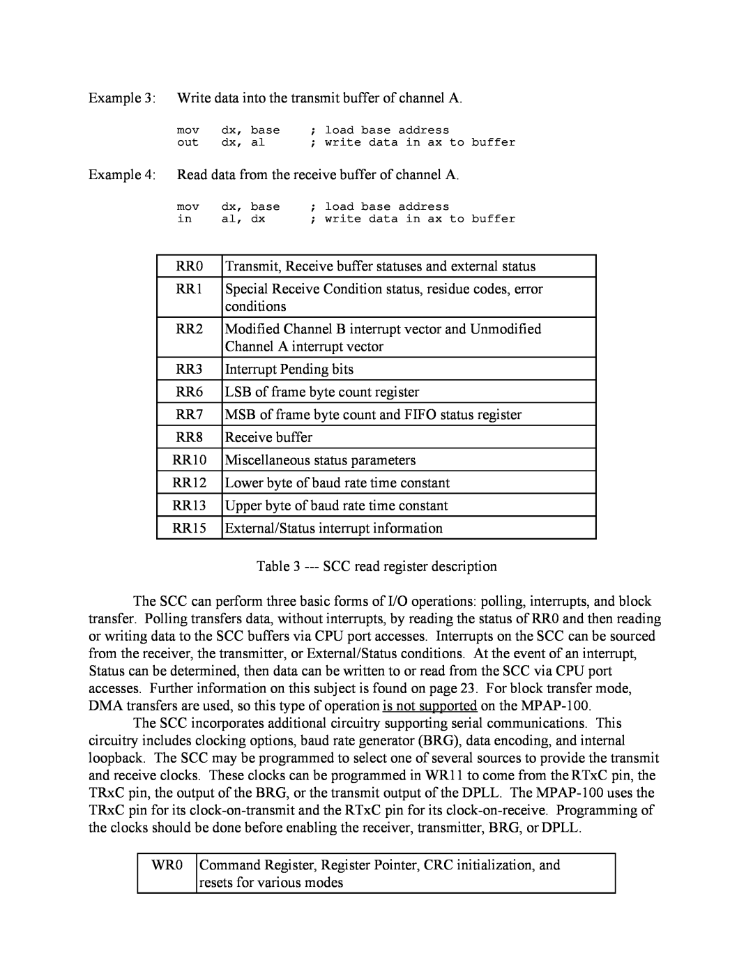
9 SCC General Information
SDLC/HDLC Bit Synchronous Communications
Byte-oriented Synchronous Communications
9.1 Accessing the registers
Example 3 Write data into the transmit buffer of channel A
Interrupt vector
Master interrupt control and reset
coding, CRC reset
Interrupt control, Wait/DMA request control
ClockFrequency TimeConst 2 BaudRate ClockMode
9.2 Baud Rate Generator Programming
9.3 SCC Data Encoding Methods
9.4 Support for SCC Channel B
9.4.3 Extra handshaking for channel A
9.4.1 Receive data and clock signals
9.4.4 Other signals are not used
9.4.2 Extra clock support for channel A
9.5.1 Register Pointer Bits
9.5 SCC Incompatibility Warnings
9.5.2 Software Interrupt Acknowledge
10.2.1 Transmit FIFO
10.2 Accessing the FIFOs
10 FIFO Operation
10.1 Enabling and disabling the FIFOs
10.2.2 Receive FIFO
10.3 SCC configuration for FIFO operation
Register
10.3.2 Using channel B for receive
10.4.1 Interrupt status
10.4 FIFO status and control
10.4.4 Controlling the FIFOs
10.4.2 Resetting the FIFOs
10.5 Accessing the SCC while FIFOs are enabled
10.4.3 Reading current FIFO status
Page
10.7 Receive FIFO timeout
SWSYNC
11 Communications Register
Bit 2 TCKEN --- Transmit Clock Source
RCKEN --- Receive Clock Source
Bits 1-0 Reserved, always
External Data FIFOs Present --- Reserved, always
12 Configuration Register
INTS1, INTS0 --- Interrupt Source and Enable Bits
FIFOEN --- External data FIFO enable
RXSRC --- Receive FIFO DMA Source
13 Interrupt Status Register
14 FIFO Status Register
15 FIFO Control Register
Bits 7-0 Receive Pattern CharacterThis is
16 Receive Pattern Character Register
Bits 7-0 Receive Pattern Count
17 Receive Pattern Count Register
Bit 6 Reserved, always Bits 5-0 Timeout Interval
18 Receive FIFO Timeout Register
Bit 7 X16MODE --- Clock Mode
19 External Connections
19.2 RING pin
19.1 SYNCA pin
19.3 Null-modem cables
CIRCUIT CB - CLEAR TO SEND
20 DTE Interface Signals
CIRCUIT AB - SIGNAL GROUND
CIRCUIT BB - RECEIVED DATA
CIRCUIT CF - RECEIVED LINE SIGNAL DETECT CARRIER DETECT
CIRCUIT CC - DCE READY DATA SET READY CONNECTOR NOTATION DSR
CIRCUIT CD - DTE READY DATA TERMINAL READY CONNECTOR NOTATION DTR
CIRCUIT CE - RING INDICATOR CONNECTOR NOTATION RING
CIRCUIT TM - TEST MODE
21 Specifications
22.1 DOS Client Driver 22.1.1 Generic SuperClient Drivers
22 Software Troubleshooting
22.1.3 Multiple Configuration Attempts
22.2 DOS Enabler
22.3 OS/2 Client Driver 22.3.1 Resources Not Available
22.2.1 With Card and Socket Services
22.2.2 Socket Numbers
22.2.3 Memory range exclusion
Page
MPAP-100 Users Manual Revision March P/N