Circuit Descriptions
12-1) POWER BUS
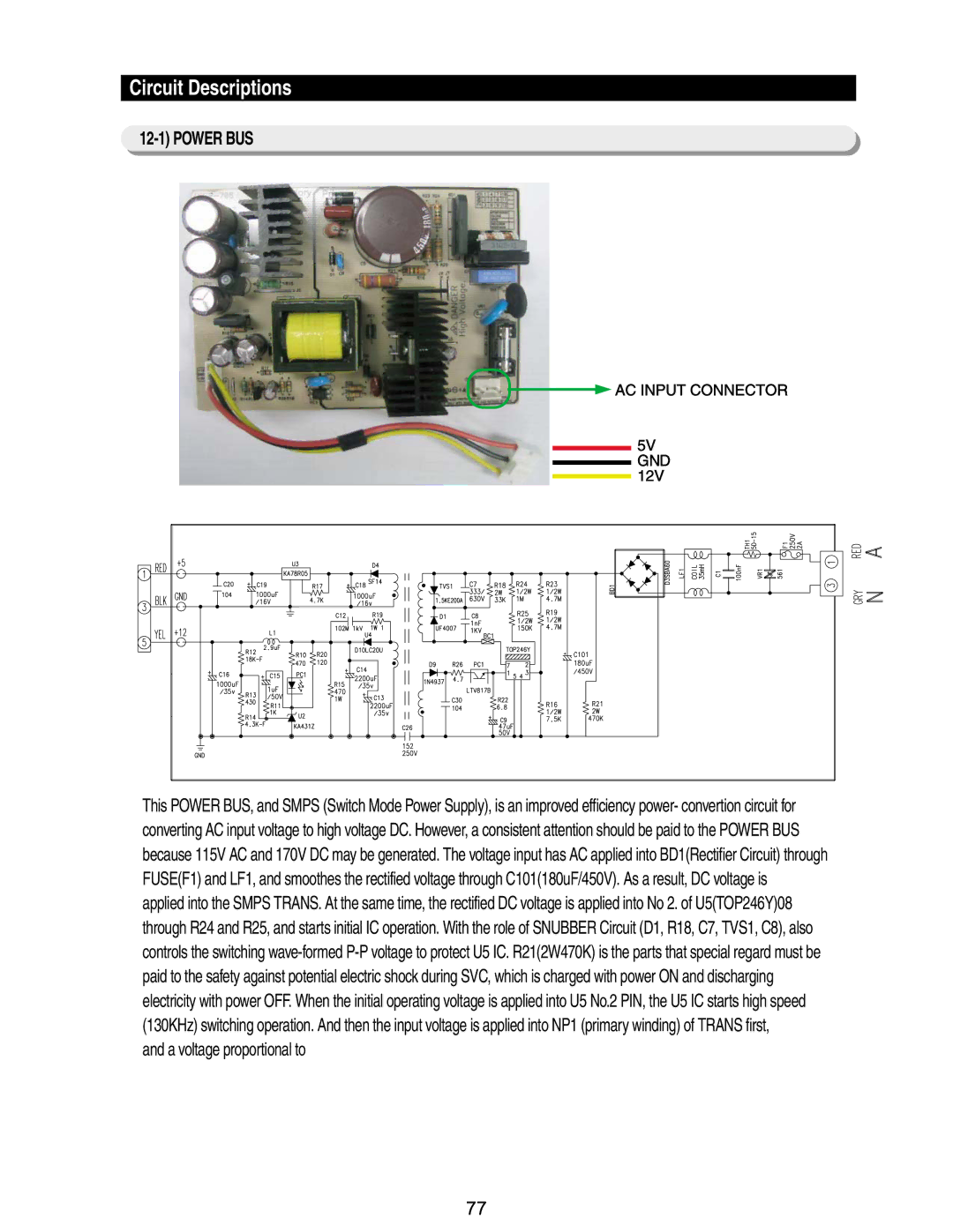
This POWER BUS, and SMPS (Switch Mode Power Supply), is an improved efficiency power- convertion circuit for converting AC input voltage to high voltage DC. However, a consistent attention should be paid to the POWER BUS because 115V AC and 170V DC may be generated. The voltage input has AC applied into BD1(Rectifier Circuit) through FUSE(F1) and LF1, and smoothes the rectified voltage through C101(180uF/450V). As a result, DC voltage is applied into the SMPS TRANS. At the same time, the rectified DC voltage is applied into No 2. of U5(TOP246Y)08 through R24 and R25, and starts initial IC operation. With the role of SNUBBER Circuit (D1, R18, C7, TVS1, C8), also controls the switching
and a voltage proportional to
77