S3C9228/P9228
S3C9228/P9228
Important Notice
Preface
Page
Table of Contents
Chapter Control Registers
Part II Hardware Descriptions
Chapter Timer
Table of Contents Concluded
Page
List of Figures
Title Number
Xii
10-4
List of Figures Concluded
List of Tables
Page
Clock Circuits
Description Number Address Spaces
Interrupt Structure
Page
List of Register Descriptions
Register Full Register Name Identifier Number
Page
List of Instruction Descriptions
Instruction Full Instruction Name Mnemonic Number
Product Overview
CPU
Block Diagram
44-QFP
S3C9228 44-QFP Pin Assignments
S3C9228 42-SDIP
S3C9228 42-SDIP Pin Assignments
PIN Descriptions
XTOUT, Xtin
PIN Circuit Diagrams
Pin Circuit Type E-4
Pin Circuit Type H-23
10. Pin Circuit Type H-32
12. Pin Circuit Type H-32B
Address Spaces
Program Memory ROM
Register Architecture
Common Working Register Area C0H-CFH
Stack Operations
Stack Pointer SP
Push SYM
Addressing Modes
Register Addressing Mode R
Register Addressing
Indirect Register Addressing Mode IR
Indirect Register Addressing to Register File
Indirect Register Addressing Mode
Indirect Register Addressing to Program Memory
Indirect Working Register Addressing to Register File
Indirect Register Addressing Mode Concluded
Indexed Addressing Mode
Indexed Addressing to Register File
Indexed Addressing Mode
Indexed Addressing Mode Concluded
Direct Address Mode DA
10. Direct Addressing for Load Instructions
Direct Address Mode
11. Direct Addressing for Call and Jump Instructions
Relative Address Mode RA
Immediate Mode IM
Control Registers
Hex
BAH
Bit Identifier Reset Value Read/Write
Flags System Flags Register
Adcon A/D Converter Control Register
D0H
Btcon Basic Timer Control Register
Basic Timer Input Clock Selection Bits
Basic Timer Counter Clear Bit
DCH
Clkcon System Clock Control Register
D4H
Bits
CPU Clock System Clock Selection Bits
Flags System Flags Register
D5H
INTPND1 Interrupt Pending Register
D6H
INTPND2 Interrupt Pending Register
D7H
Lmod LCD Mode Control Register
FEH
Lpot LCD Port Control Register
D8H
Osccon Oscillator Control Register
D3H
Main Oscillator Control Bit
Sub Oscillator Control Bit
P0.2/INT Configuration Bits
P0.1/T1CLK/INT Configuration Bits
P0.0/TAOUT/INT Configuration Bits
P0CON Port 0 Control Register
P0INT -Port 0 Interrupt Enable Register
EDH
P0PUR -Port 0 Pull-up Resistors Enable Register
ECH
P0EDGE -Port 0 Interrupt Edge Selection Register
EEH
P1.2/AD2/INT Configuration Bits
P1.1/AD1/INT Configuration Bits
P1.0/AD0/INT Configuration Bits
P1CON Port 1 Control Register
P1INT -Port 1 Interrupt Enable Register
F1H
P1PUR -Port 1 Pull-up Resistors Enable Register
F0H
P1EDGE -Port 1 Interrupt Edge Selection Register
F2H
P2.2/SI Configuration Bits
P2.1/SO Configuration Bits
P2.0/SCK Configuration Bits
P2CON Port 2 Control Register
P2PUR -Port 2 Pull-up Resistors Enable Register
F4H
P3.1/SEG2/INTP Configuration Bits
P3.0/SEG3/INTP Configuration Bits
P3CON Port 3 Control Register
F5H
P3INT -Port 3 Interrupt Enable Register
P3.1s Interrupt Enable Bit
P3.0s Interrupt Enable Bit
F7H
P3PUR -Port 3 Pull-up Resistors Enable Register
P3.1s Pull-up Resistor Enable Bit
P3.0s Pull-up Resistor Enable Bit
F6H
P3.1s Interrupt State Setting Bit
P3.0s Interrupt State Setting Bit
P3EDGE -Port 3 Interrupt Edge Selection Register
F8H
P4.6/SEG10 Configuration Bits
P4.5/SEG9 Configuration Bits
P4.4/SEG8 Configuration Bits
P4CONH Port 4 Control Register High Byte
P4.2/SEG6 Configuration Bits
P4.1/SEG5 Configuration Bits
P4.0/SEG4 Configuration Bits
P4CONL-Port 4 Control Register Low Byte
P5.6/SEG18/COM5 Configuration Bits
P5.5/SEG17/COM6 Configuration Bits
P5.4/SEG16/COM7 Configuration Bits
P5CONH Port 5 Control Register High Byte
P5.2/SEG14 Configuration Bits
P5.1/SEG13 Configuration Bits
P5.0/SEG12 Configuration Bits
P5CONL Port 5 Control Register Low Byte
P6.2/COM1 Configuration Bits
P6.1/COM2 Configuration Bits
P6.0/COM3 Configuration Bits
P6CON Port 6 Control Register High Byte
Siocon SIO Control Register
E1H
E0H
Bit Identifier Reset Value Read/Write Stop Control Bits
Stpcon Stop Control Register
SYM System Mode Register
Global Interrupt Enable Bit
DFH
Selection Bits
Tacon Timer 1/A Control Register
BBH
Tbcon Timer B Control Register
BAH
Wtcon Watch Timer Control Register
DAH
ENABLE/DISABLE Interrupt Instructions EI, DI
Interrupt Processing Control Points
Interrupt Pending Function Types
Interrupt Priority
Generating Interrupt Vector Addresses
Interrupt Source Service Sequence
Interrupt Service Routines
S3C9228/P9228 Interrupt Structure
S3C9228/P9228 Interrupt Structure
Programming Tip How to clear an interrupt pending bit
Examples
Register Addressing
Addressing Modes
Instruction Group Summary
Mnemonic Operands Instruction Load Instructions
Arithmetic Instructions
Logic Instructions
CPU Control Instructions
Bit Manipulation Instructions
Rotate and Shift Instructions
Flags Register Flags
Flag Descriptions
Instruction Set Symbols
Symbol Description
Instruction SET Notation
Flag Notation Conventions
IRR
Opcode Quick Reference
Opcode MAP Lower Nibble HEX
INC NOP
Condition Codes
Condition Codes Binary Mnemonic Description Flags Set
Instruction Descriptions
Flags
Format Bytes Cycles Opcode Addr Mode Hex Dst Src
ADC Add With Carry
ADD Add
Logical
Call Call Procedure
Bytes Cycles Opcode Addr Mode Hex Dst
Call
Operation
CCF Complement Carry Flag
CCF
Format Bytes Cycles Opcode Hex
Example
CLRdst Operation dst ¨
Format Bytes Cycles Opcode Addr Mode Hex Dst
CLR Clear
COM Complement
COMdst
CP Compare
INC Skip
DEC Decrement
DEC
DI Disable Interrupts
Operation SYM 2 ¨
EI Enable Interrupts
Idle Idle Operation
Idle
INC Increment
INCdst
Iret Interrupt Return
Iretiret
Operation Flags ¨ @SP
Iret
JP Jump
Labelw
Bytes Cycles Opcode Addr Mode Hex Dst CcB
JR Jump Relative
LD Load
SAM88RI Instruction SET
LDC/LDE dst,src Operation dst ¨ src
Bytes Cycles Opcode Addr Mode Hex Dst Src
LDC/LDE Load Memory
LDC note
LDCD/LDED dst,src Operation dst ¨ src
Bytes Cycles Opcode Addr Mode Hex Dst Src Irr
LDCD/LDED Load Memory and Decrement
LDCI/LDEI Load Memory and Increment
LDCI/LDEI dst,src Operation dst ¨ src
NOP No Operation
NOP
Or Logical or
POP Pop From Stack
POPdst Operation dst ¨ @SP
Push Push To Stack
PUSHsrc Operation SP ¨ SP
RCF Reset Carry Flag
RCF
Operation PC ¨ @SP
RET Return
RET
RL Rotate Left
Operation ¨ dst
RLC Rotate Left Through Carry
RLCdst Operation dst 0 ¨ C
RR Rotate Right
RRC Rotate Right Through Carry
RRCdst Operation dst 7 ¨ C
SBC Subtract With Carry
SBC
SCF Set Carry Flag
SCF
SRA Shift Right Arithmetic
SRA
Stop Stop Operation
Stop
SUB Subtract
SUB
TCM Test Complement Under Mask
TM Test Under Mask
Operation dst and src
XOR Logical Exclusive or
System Clock Circuit
CPU Clock Notation
Main Oscillator Circuits
SUB Oscillator Circuits
Clock Status During POWER-DOWN Modes
System Clock Circuit Diagram
System Clock Control Register Clkcon
System Clock Control Register Clkcon
Oscillator Control Register Osccon
Oscillator Control Register Osccon
Switching the CPU Clock
+PROGRAMMING TIP Switching the CPU clock
Stop Control Register Stpcon
Clock Circuits
Reset and POWER-DOWN
Overview
Using an External Interrupt to Release Stop Mode
Stop Mode
Using Reset to Release Stop Mode
Idle Mode Release
Using an Internal Interrupt to Release Stop Mode
Idle Mode
Hardware Reset Values
Port 0 Pull-up Resistors Enable Register
Reset and POWER-DOWN S3C9228/P9228
S3C9228 Port Configuration Overview Configuration Options
O Ports
Port Data Registers
S3C9228 I/O Port Data Register Format
Port 0 Pull-up Resistor Control Register P0PUR
Port
Port 0 Control register P0CON
Port 0 Interrupt Control Register P0INT
Port 0 Interrupt Pending Bits INTPND1.3-.0
Port 1 Control Register P1CON
Port 1 Pull-up Resistor Control Register P1PUR
Port 1 Interrupt Control Register P1INT
10. Port 1 Interrupt Edge Selection Register P1EDGE
Port 2 Control Register P2CON
Port 2 Pull-up Resistor Control Register P2PUR
13. Port 2 Pull-up Control Register P2PUR
Port 3 Control Register P3CON
Port 3 Pull-up Resistor Control Register P3PUR
15. Port 3 Interrupt Control Register P3INT
17. Port 3 Interrupt Edge Selection Register P3EDGE
Port 4 Control Registers P4CONH, P4CONL
19. Port 4 High-Byte Control Register P4CONH
Port 5 Control Registers P5CONH, P5CONL
21. Port 5 High-Byte Control Register P5CONH
Port 6 Control Register P6CON
23. Port 6 Control Register P6CON
Basic Timer
Basic Timer Control Register Btcon
Basic Timer Control Register Btcon
Oscillation Stabilization Interval Timer Function
Basic Timer Function Description
Watchdog Timer Function
Basic Timer Block Diagram
Interval Timer Function
Function Description
Timer 1 Control Register Tacon
BBH, R/W MSB LSB
Timer 1 Block Diagram One 16-bit Mode
TWO 8-BIT Timers Mode Timer a and B
Timer a and B Control Register TACON, Tbcon
Timer a Control Register Tacon
Timer B Control Register Tbcon
Interval Timer Function Timer a and Timer B
Timer a Block DiagramTwo 8-bit Timers Mode
Timer B Block Diagram Two 8-bit Timers Mode
11-10
Watch Timer
Watch Timer Control Register Wtcon
Watch Timer Control Register Wtcon
Watch Timer Circuit Diagram
12-4
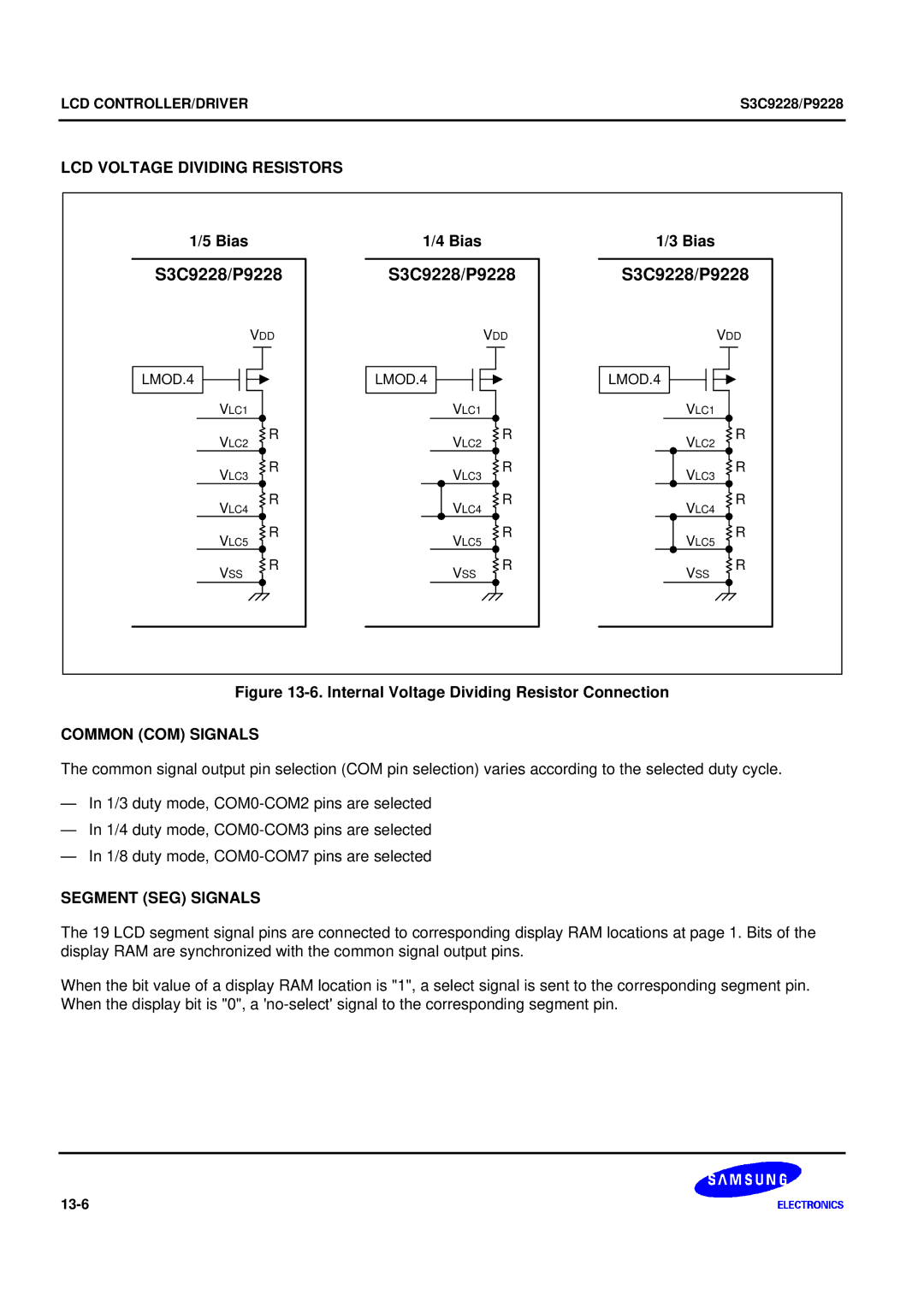
LCD CONTROLLER/DRIVER
LCD Circuit Diagram
LCD Circuit Diagram
LCD RAM Address Area
SEG0 SEG1 SEG2 SEG3 SEG17 SEG18 SEG19
LCD Mode Control Register Lmod
LCD Mode Control Register Lmod
LCD Port Control Register
LCD Port Control Register
Common COM Signals
Segment SEG Signals
LCD Voltage Dividing Resistors
Bias
LCD Signal Waveforms 1/8 Duty, 1/4 Bias
LCD Signal Waveforms 1/4 Duty, 1/3 Bias
LCD Signal Waveforms 1/3 Duty, 1/3 Bias
13-10
14 10-BIT ANALOG-TO-DIGITAL Converter
Conversion Timing
Converter Control Register Adcon
A/D Converter Data Register ADDATAH/ADDATAL
Internal Reference Voltage Levels
S3C9228
Programming Procedure
Serial I/O Interface
SIO Control Registers Siocon
Serial I/O Module Control Register Siocon
SIO PRE-SCALER Register Siops
SIO Prescaler Register Siops
Serial I/O Timing Diagram SIO
Electrical Data
Parameter Symbol Conditions Rating Unit
D.C. Electrical Characteristics
Parameter Symbol Conditions Min Typ Max Unit
Absolute Maximum Ratings
XOUT, XTIN, Xtout
D.C. Electrical Characteristics Concluded
Data Retention Supply Voltage in Stop Mode
~ ~ ~ ~
TA = 25 C, VDD = 0
A.C. Electrical Characteristics
A/D Converter Electrical Characteristics
Input Timing for External Interrupts
Input Timing for Reset
Units
Main Oscillation Characteristics
Sub Oscillation Characteristics
Main Oscillation Stabilization Time
Oscillator Test Condition Min Typ Max Unit
10. Sub Oscillation Stabilization Time
Clock Timing Measurement at Xtin
16-13
16-14
Mechanical Data
QFP-1010B
18 S3P9228 OTP
S3P9228 42-SDIP Pin Assignments
Operating Mode Characteristics
PP Test REG/MEM
18-4
Standard Operating Voltage Range
S3P9228 OTP S3C9228/P9228 18-6
Shine
Sama Assembler
SASM86
HEX2ROM
Smds Product Configuration SMDS2+
SM1347A
TB9228 Target Board
Power Selection Settings for TB9228
To UserV CC Operating Mode Comments Settings
SMDS2+ Tool Selection Setting SW1 Setting Operating Mode
SMDS2+ Selection SAM8
Idle LED
Stop LED
Connectors J101, J102 for TB9228
S3C9228 Probe Adapter for 42-SDIP Package
19-8
Product Overview
Features
Block Diagram
S3C9228
S3C9228 42-SDIP
PIN Descriptions
VDD, VSS
PIN Circuit Diagrams
Pin Circuit Type E-4
Pin Circuit Type H-23
10. Pin Circuit Type H-32
12. Pin Circuit Type H-32B
Address Spaces
Program Memory ROM
Register Architecture
Common Working Register Area C0H-CFH
System Stack
Push SYM
Addressing Modes
Register Addressing Mode R
Indirect Register Addressing Mode IR
Indirect Register Addressing to Program Memory
Indirect Working Register Addressing to Register File
Indirect Register Addressing Mode Concluded
Indexed Addressing Mode
Indexed Addressing Mode
Indexed Addressing Mode Concluded
Direct Address Mode DA
11. Direct Addressing for Call and Jump Instructions
Relative Address Mode RA
Control Registers
Hex
Tbcon
Register Description Format
Adcon A/D Converter Control Register
Btcon Basic Timer Control Register
Clkcon System Clock Control Register
Flags System Flags Register
INTPND1 Interrupt Pending Register
INTPND2 Interrupt Pending Register
Lmod LCD Mode Control Register
Lpot LCD Port Control Register
Osccon Oscillator Control Register
P0CON Port 0 Control Register
P0INT -Port 0 Interrupt Enable Register
P0PUR -Port 0 Pull-up Resistors Enable Register
P0EDGE -Port 0 Interrupt Edge Selection Register
P1CON Port 1 Control Register
P1INT -Port 1 Interrupt Enable Register
P1PUR -Port 1 Pull-up Resistors Enable Register
P1EDGE -Port 1 Interrupt Edge Selection Register
P2CON Port 2 Control Register
P2PUR -Port 2 Pull-up Resistors Enable Register
P3CON Port 3 Control Register
P3INT -Port 3 Interrupt Enable Register
P3PUR -Port 3 Pull-up Resistors Enable Register
P3EDGE -Port 3 Interrupt Edge Selection Register
P4CONH Port 4 Control Register High Byte
FAH
P5CONH Port 5 Control Register High Byte
P5CONL Port 5 Control Register Low Byte
P6CON Port 6 Control Register High Byte
Siocon SIO Control Register
Stpcon Stop Control Register
SYM System Mode Register
Tacon Timer 1/A Control Register
Tbcon Timer B Control Register
Wtcon Watch Timer Control Register
Interrupt Structure
Interrupt Pending Function Types
Interrupt Source Service Sequence
S3C9228/P9228 Interrupt Structure
S3C9228/P9228 Interrupt Structure
Programming Tip How to clear an interrupt pending bit
SAM88RCRI Instruction SET
Instruction Group Summary
Bit Manipulation Instructions
Flags Register Flags
Instruction SET Notation
IRR
Opcode MAP Lower Nibble HEX
Idle
Condition Codes
Instruction Descriptions
ADC Add With Carry
ADD Add
Logical
Call Call Procedure
CCF Complement Carry Flag
CLR Clear
COM Complement
CP Compare
DEC Decrement
DI Disable Interrupts
EI Enable Interrupts
Idle Idle Operation
INC Increment
Iret Interrupt Return
JP Jump
JR Jump Relative
LD Load
SAM88RI Instruction SET
LDC/LDE Load Memory
LDC
LDCD/LDED Load Memory and Decrement
LDCI/LDEI Load Memory and Increment
NOP No Operation
Or Logical or
POP Pop From Stack
Push Push To Stack
RCF Reset Carry Flag
RET Return
RL Rotate Left
RLC Rotate Left Through Carry
RR Rotate Right
RRC Rotate Right Through Carry
SBC Subtract With Carry
SCF Set Carry Flag
SRA Shift Right Arithmetic
Stop Stop Operation
SUB Subtract
TCM Test Complement Under Mask
TM Test Under Mask
XOR Logical Exclusive or
Clock Circuits
Main Oscillator Circuits
Clock Status During POWER-DOWN Modes
System Clock Control Register Clkcon
Oscillator Control Register Osccon
Switching the CPU Clock
Stop Control Register Stpcon
Clock Circuits
Reset and POWER-DOWN
POWER-DOWN Modes
Idle Mode
Hardware Reset Values
SYM
Reset and POWER-DOWN S3C9228/P9228
O Ports
Port Data Registers
Port
Port 0 Interrupt Control Register P0INT
Port 0 Interrupt Pending Bits INTPND1.3-.0
Port
Port 1 Interrupt Control Register P1INT
10. Port 1 Interrupt Edge Selection Register P1EDGE
Port
13. Port 2 Pull-up Control Register P2PUR
14. Port 3 Control Register P3CON
15. Port 3 Interrupt Control Register P3INT
17. Port 3 Interrupt Edge Selection Register P3EDGE
Port
21. Port 5 High-Byte Control Register P5CONH
23. Port 6 Control Register P6CON
Basic Timer
Basic Timer Control Register Btcon
Basic Timer Function Description
Basic Timer Block Diagram
Timer
Timer 1 Control Register Tacon
Timer 1 Block Diagram One 16-bit Mode
TWO 8-BIT Timers Mode Timer a and B
Timer a Control Register Tacon
Timer B Control Register Tbcon
Function Description
Timer a Block DiagramTwo 8-bit Timers Mode
Timer B Block Diagram Two 8-bit Timers Mode
11-10
Watch Timer
Watch Timer Control Register Wtcon
Watch Timer Circuit Diagram
12-4
LCD CONTROLLER/DRIVER
LCD Circuit Diagram
LCD RAM Address Area
LCD Mode Control Register Lmod
LCD Port Control Register
S3C9228/P9228
LCD Signal Waveforms 1/8 Duty, 1/4 Bias
LCD Signal Waveforms 1/4 Duty, 1/3 Bias
LCD Signal Waveforms 1/3 Duty, 1/3 Bias
13-10
14 10-BIT ANALOG-TO-DIGITAL Converter
Conversion Timing
Block Diagram
S3C9228
Serial I/O Interface
SIO Control Registers Siocon
SIO Block Diagram
Serial I/O Timing Diagram SIO
Electrical Data
Absolute Maximum Ratings
XOUT, XTIN, Xtout
D.C. Electrical Characteristics Concluded
~ ~ ~ ~
TA = 25 C, VDD = 0
A.C. Electrical Characteristics
Input Timing for External Interrupts
Input Timing for Reset
Main Oscillation Characteristics
Clock Timing Measurement at XIN
Clock Timing Measurement at Xtin
Operating Voltage Range
16-14
Mechanical Data
QFP-1010B
18 S3P9228 OTP
S3C9228 42-SDIP
Operating Mode Characteristics
D.C. Electrical Characteristics
Standard Operating Voltage Range
S3P9228 OTP S3C9228/P9228 18-6
Development Tools
Smds Product Configuration SMDS2+
TB9228
Power Selection Settings for TB9228
Idle LED
Connectors J101, J102 for TB9228
S3C9228 Probe Adapter for 42-SDIP Package
19-8