![]()
![]()
![]()
![]() X7DBU/X7DGU User's Manual
X7DBU/X7DGU User's Manual
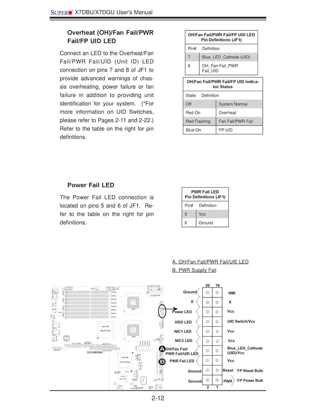
Overheat (OH)/Fan Fail/PWR Fail/FP UID LED
Connect an LED to the Overheat/Fan Fail/PWR Fail/UID (Unit ID) LED connection on pins 7 and 8 of JF1 to provide advanced warnings of chas- sis overheating, power failure or fan failure in addition to providing unit identification for your system. (*For more information on UID Switches, please refer to Pages
OH/Fan Fail/PWR Fail/FP UID LED
Pin Definitions (JF1)
Pin# Definition
7Blue_LED_Cathode (UID)
8OH_Fan Fail_PWR Fail_UID
OH/Fan Fail/PWR Fail/FP UID Indica-
tor Status
State Definition
Off | System Normal | |
Red On | Overheat | |
Red Flashing | Fan Fail/PWR Fail | |
|
| |
Blue On | FP UID | |
|
|
Power Fail LED
The Power Fail LED connection is located on pins 5 and 6 of JF1. Re- fer to the table on the right for pin definitions.
PWR Fail LED
Pin Definitions (JF1)
Pin# Definition
5Vcc
6Ground
A.OH/Fan Fail/PWR Fail/UIE LED
B.PWR Supply Fail
|
|
|
|
|
|
|
| Fan7 | 71 |
|
|
|
|
|
|
|
|
|
| Buzzer |
|
| J |
|
|
|
|
|
|
| Fan6 | Fan5 |
|
| PWR SMB |
|
|
|
| ||
|
|
|
| SP1 |
| CPU Fan1 |
|
|
|
|
| ||
JKM1 |
|
|
|
|
|
| DIMM4B |
|
|
|
|
| |
KB/MS0/1USB COM1 |
| Bank3Bank4 | J9B1J9B2 J8B2J8B3 J8B1 |
|
|
|
| DIMM4A |
|
|
|
|
|
|
|
|
|
| DIMM3B |
|
|
|
|
| |||
|
|
|
|
| DIMM3A |
|
|
|
|
| |||
|
|
|
|
| DIMM2B |
|
|
|
|
| |||
JCOM1 | Bank2 | J7B3 |
|
|
|
| DIMM2A |
| CPU1 |
|
|
| |
|
|
|
|
|
|
|
|
| |||||
|
|
|
|
|
|
|
|
|
|
|
| ||
| Battery | J7B2 |
|
|
|
| DIMM1B |
|
|
|
|
| |
|
| Bank1 |
|
|
|
|
|
|
|
|
| ||
VGA |
| J7B1 |
|
|
|
| DIMM1A |
|
|
|
|
| |
|
|
|
|
|
|
|
|
|
|
| |||
J15 |
|
|
|
|
|
|
|
|
|
|
|
|
|
LAN1 |
|
|
|
|
|
| Intel 5000 |
|
|
|
|
| |
JLAN1 |
|
|
|
|
|
|
|
|
|
|
| ||
|
|
|
|
|
|
|
|
|
|
|
|
| |
LAN2 |
|
|
|
|
|
| (North Bridge) |
|
|
|
|
| |
|
|
|
|
|
|
|
|
|
|
|
|
| |
JLAN2 |
|
|
|
|
|
|
|
|
|
|
|
|
|
| UID |
| LAN |
|
|
|
|
|
| CPU2 |
|
|
|
|
|
|
|
|
|
|
|
|
|
|
|
| |
LE2 SW1 | Rear |
| CTRL |
|
|
|
|
|
|
|
|
|
|
|
|
| I2C2 | I2C1 |
|
|
|
| 1AT AS- I | 2AT AS- I | 3AT AS- I | ||
| J14 | J28 | J27 | SXB2: |
|
| |||||||
|
|
|
|
| 9J |
| 0 | ||||||
UIO PWR | J11 |
|
|
|
|
| SXB1: | 5J | ATSA |
|
|
| |
|
|
|
|
|
| X7DBU |
|
|
|
|
| ||
|
|
|
|
|
|
|
|
|
|
|
| ||
|
|
|
|
|
|
|
|
|
|
| SGPIO1 |
|
|
|
|
|
|
|
|
|
|
| Intel ESB2 | J29 |
|
| |
|
|
|
|
|
|
|
|
| J30 |
|
| ||
|
|
|
|
|
|
|
|
|
|
|
| ||
|
|
|
|
|
|
|
|
|
|
| SGPIO2 |
|
|
|
|
|
|
|
|
|
|
| (South Bridge) |
|
|
|
|
|
|
|
|
|
|
|
|
|
|
| SIO B |
|
|
| 20 | 19 | ||
2W PJ | 3W PJ |
| Ground |
|
1W PJ |
|
|
| |
|
|
|
| |
|
| Fan1 | X |
|
|
| JF1 |
|
|
|
| TRLCFP | Power LED |
|
|
| |
| Fan2 |
|
|
|
| 1DJ | HDD LED |
| LE1 | ||
| JOH1 |
| |
|
| JP1 |
|
|
|
| NIC1 LED |
|
| Fan3 |
|
| Fan8 |
| NIC2 LED |
4AT | CPU FAN2 |
| |
5AT | A OH/Fan Fail/ | ||
|
| ||
|
| 1E# ID | PWR Fail/UID LED |
| SIMSO | B PWR Fail LED | |
NMI
X
Vcc
UID Switch/Vcc
Vcc
Vcc
Blue_LED_Cathode (UID)/Vcc
Vcc
| JBT1 | ry |
|
JWOR1 | J7 | Memoideo |
|
JPG1 |
|
| |
ES1000 |
|
| |
|
| V |
|
Video CTRL |
| JWD | O |
|
| JK1 | I/ |
|
|
| S |
COM2 |
| JWOL1 |
|
| JPL1 | JPL2 | USB4 |
|
|
|
Floppy | Ground | Reset FP Reset Butto |
| J18 | Ground | PWR | FP Power Butt |
SMB | J22 |
JL1 | 2 | 1 |
Fan4 | ||
USB2/3 |
|
|