![]()
![]()
![]()
![]() X7DBU/X7DGU User's Manual
X7DBU/X7DGU User's Manual
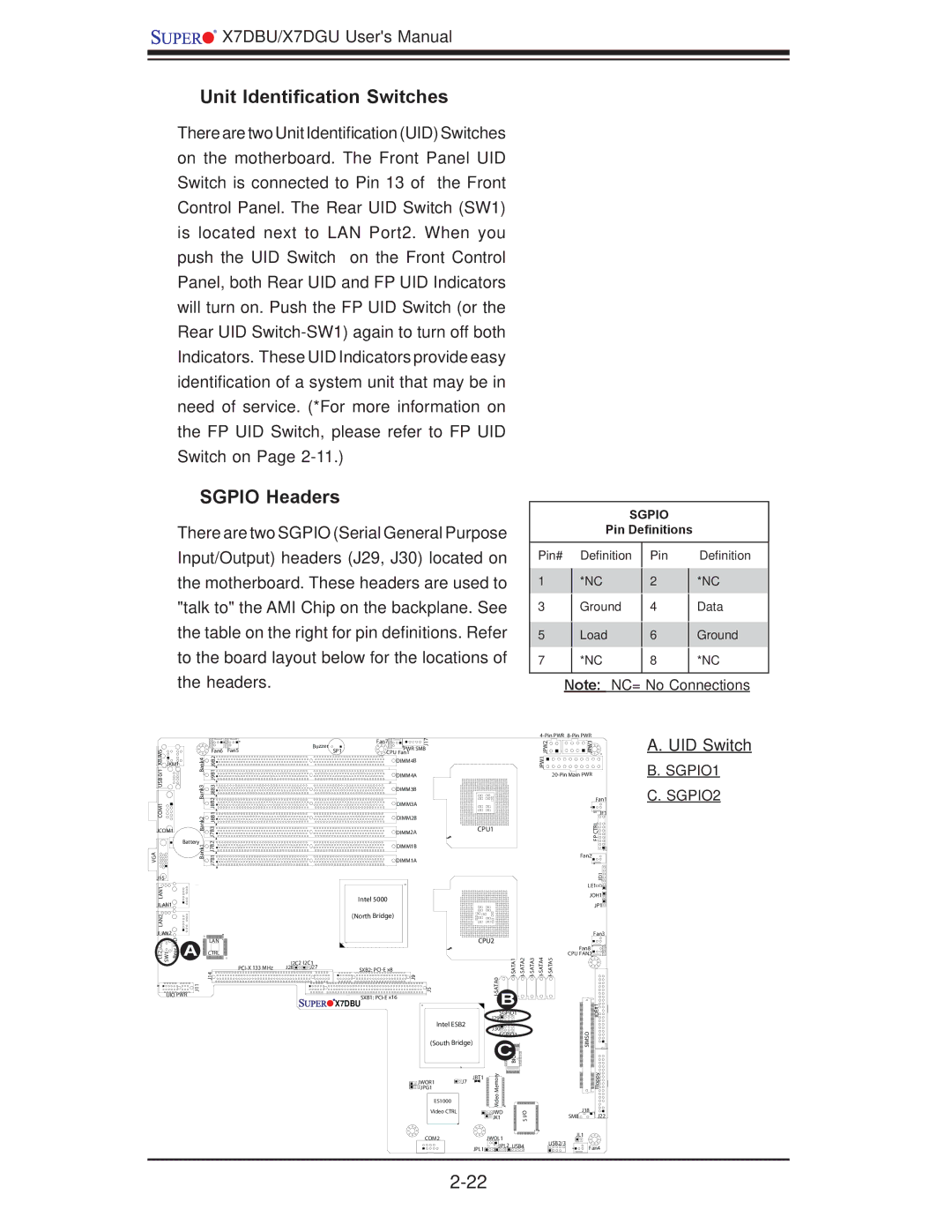
Unit Identification Switches
There are two Unit Identification (UID) Switches on the motherboard. The Front Panel UID Switch is connected to Pin 13 of the Front Control Panel. The Rear UID Switch (SW1) is located next to LAN Port2. When you push the UID Switch on the Front Control Panel, both Rear UID and FP UID Indicators will turn on. Push the FP UID Switch (or the Rear UID
SGPIO Headers
There are two SGPIO (Serial General Purpose Input/Output) headers (J29, J30) located on the motherboard. These headers are used to "talk to" the AMI Chip on the backplane. See the table on the right for pin definitions. Refer to the board layout below for the locations of the headers.
SGPIO
Pin Definitions
Pin# |
| Definition | Pin |
| Definition |
1 |
| *NC | 2 |
| *NC |
|
| ||||
3 |
| Ground | 4 |
| Data |
|
| ||||
5 |
| Load | 6 |
| Ground |
|
| ||||
7 |
| *NC |
|
| *NC |
| 8 |
| |||
|
|
|
|
|
|
Note: NC= No Connections
|
|
| Fan6 | Fan5 |
| SP1 |
| CPU Fan1 | 17 |
|
|
|
|
|
|
| A. UID Switch | ||
|
|
|
|
|
|
|
|
|
|
| 2PWJ | 3PWJ |
| ||||||
|
|
|
|
|
|
|
| Fan7 |
|
|
|
|
|
|
|
|
|
| |
|
|
|
|
|
| Buzzer |
|
| J |
|
|
|
|
|
|
|
|
|
|
KB/MS0/1USBCOM1 |
|
|
|
|
|
| PWR SMB |
|
|
|
|
|
|
|
|
|
| ||
| Bank3Bank4 | J8B2J8B3J8B1J9B1J9B2 |
|
|
|
|
|
|
|
|
|
| 1PWJ |
|
|
| |||
|
|
|
|
| DIMM4B |
|
|
|
|
|
|
|
|
| B. SGPIO1 | ||||
JKM1 |
|
|
|
|
|
|
|
|
|
|
|
|
|
|
|
| |||
|
|
|
|
|
|
|
|
|
|
|
|
|
|
|
|
| |||
|
|
|
|
|
|
|
| DIMM4A |
|
|
|
|
|
|
|
|
| ||
|
|
|
|
|
|
|
| DIMM3B |
|
|
|
|
|
|
|
|
|
| C. SGPIO2 |
|
|
|
|
|
|
|
| DIMM3A |
|
|
|
|
|
|
|
|
| Fan1 | |
|
| Bank2 |
|
|
|
|
| DIMM2B |
|
|
|
|
|
|
|
|
| JF1 |
|
|
| J7B3 |
|
|
|
|
|
|
|
|
|
|
|
|
| RLCTP |
| ||
JCOM1 |
|
|
|
| DIMM2A |
|
| CPU1 |
|
|
|
|
|
| |||||
|
| Battery | J7B2 |
|
|
|
|
|
|
|
|
|
|
|
|
|
| F |
|
VGA |
| Bank1 |
|
|
|
| DIMM1B |
|
|
|
|
|
|
|
|
|
| ||
| J7B1 |
|
|
|
|
|
|
|
|
|
|
|
|
|
|
| |||
|
|
|
|
| DIMM1A |
|
|
|
|
|
|
|
| Fan2 |
|
| |||
|
|
|
|
|
|
|
|
|
|
|
|
|
|
|
|
|
|
| |
J15 |
|
|
|
|
|
|
|
|
|
|
|
|
|
|
|
|
| 1DJ |
|
LAN1 |
|
|
|
|
|
|
|
|
|
|
|
|
|
|
|
| LE1 |
| |
|
|
|
|
|
| Intel 5000 |
|
|
|
|
|
|
|
| JOH1 |
| |||
JLAN1 |
|
|
|
|
|
|
|
|
|
|
|
|
|
|
| JP1 |
| ||
|
|
|
|
|
|
|
|
|
|
|
|
|
|
|
|
|
| ||
LAN2 |
|
|
|
|
|
| (North Bridge) |
|
|
|
|
|
|
|
|
|
|
| |
|
|
|
|
|
|
|
|
|
|
|
|
|
|
|
|
|
|
| |
JLAN2 | UID |
|
|
|
|
|
|
|
|
|
|
|
|
|
|
|
| Fan3 |
|
| A | LAN |
|
|
|
|
|
|
| CPU2 |
|
|
|
|
|
|
| ||
|
|
|
|
|
|
|
|
|
|
|
|
|
|
|
| ||||
LE2 SW1 | Rear | J14 |
|
|
|
| 9J |
|
|
| 0 | Fan8 |
|
| |||||
|
|
|
|
|
|
|
|
| |||||||||||
|
| CTRL |
|
|
|
|
|
|
|
|
|
|
|
|
| CPU FAN2 |
|
| |
|
|
|
| I2C2 | I2C1 |
|
|
|
|
|
|
|
|
|
|
|
|
| |
|
|
|
| J28 | J27 | SXB2: |
|
|
|
|
|
|
|
|
|
|
| ||
|
|
|
|
|
|
|
|
|
|
|
|
|
|
|
| ||||
|
| J11 |
|
|
| X7DBU |
| 5J |
|
|
|
|
|
| 1# |
| |||
UIO PWR |
|
|
|
|
| SXB1: |
|
|
|
|
|
|
|
|
|
|
| ||
|
|
|
|
|
|
|
|
|
|
|
|
|
|
|
|
|
|
| |
|
|
|
|
|
|
|
|
|
|
|
| SGPIO1 |
|
|
|
| E |
| |
|
|
|
|
|
|
|
|
|
|
|
|
|
|
|
| ID |
| ||
|
|
|
|
|
|
|
|
|
|
|
| J29 |
|
|
|
|
|
| |
|
|
|
|
|
|
|
|
| Intel ESB2 |
|
|
|
|
|
|
|
| ||
|
|
|
|
|
|
|
|
|
| J30 |
|
|
|
|
|
|
| ||
|
|
|
|
|
|
|
|
|
|
|
|
|
|
|
| O |
|
| |
|
|
|
|
|
|
|
|
|
|
|
| SGPIO2 |
|
|
|
|
| ||
|
|
|
|
|
|
|
|
| (South Bridge) |
| CSIOB |
|
|
| SIM |
|
| ||
|
|
|
|
|
|
|
|
|
|
|
|
|
|
| S |
|
| ||
|
|
|
|
|
|
|
|
|
|
|
|
|
|
|
| yppFlo |
| ||
|
|
|
|
|
|
|
|
| JWOR1 | J7 | JBT1 | yromeM |
|
|
|
|
|
| |
|
|
|
|
|
|
|
|
|
|
|
|
|
|
|
|
|
| ||
|
|
|
|
|
|
|
|
| JPG1 |
|
|
|
|
|
|
|
|
|
|
|
|
|
|
|
|
|
|
| ES1000 |
|
| oe |
|
|
|
|
|
|
|
|
|
|
|
|
|
|
|
|
|
| Vid |
|
|
|
|
|
|
| |
|
|
|
|
|
|
|
|
|
|
|
|
|
|
|
| J18 |
|
| |
|
|
|
|
|
|
|
|
| Video CTRL |
|
| JWD |
| I/O |
|
| J22 |
| |
|
|
|
|
|
|
|
|
|
|
|
| JK1 |
|
|
| SMB |
| ||
|
|
|
|
|
|
|
|
|
|
|
|
|
| S |
|
|
|
|
|
|
|
|
|
|
|
|
|
| COM2 |
| JWOL1 |
|
|
|
| JL1 |
|
| |
|
|
|
|
|
|
|
|
|
|
|
|
|
| USB2/3 |
|
| |||
|
|
|
|
|
|
|
|
|
|
|
| JPL2 | USB4 |
|
|
|
| ||
|
|
|
|
|
|
|
|
|
|
| JPL1 |
|
| Fan4 |
| ||||
|
|
|
|
|
|
|
|
|
|
|
|
|
|
|
|
| |||
|
|
|
|
|
|
|
|
|
|
|
|
|
|
|
|
| |||