![]()
![]()
![]() X7DBU/X7DGU User's Manual
X7DBU/X7DGU User's Manual


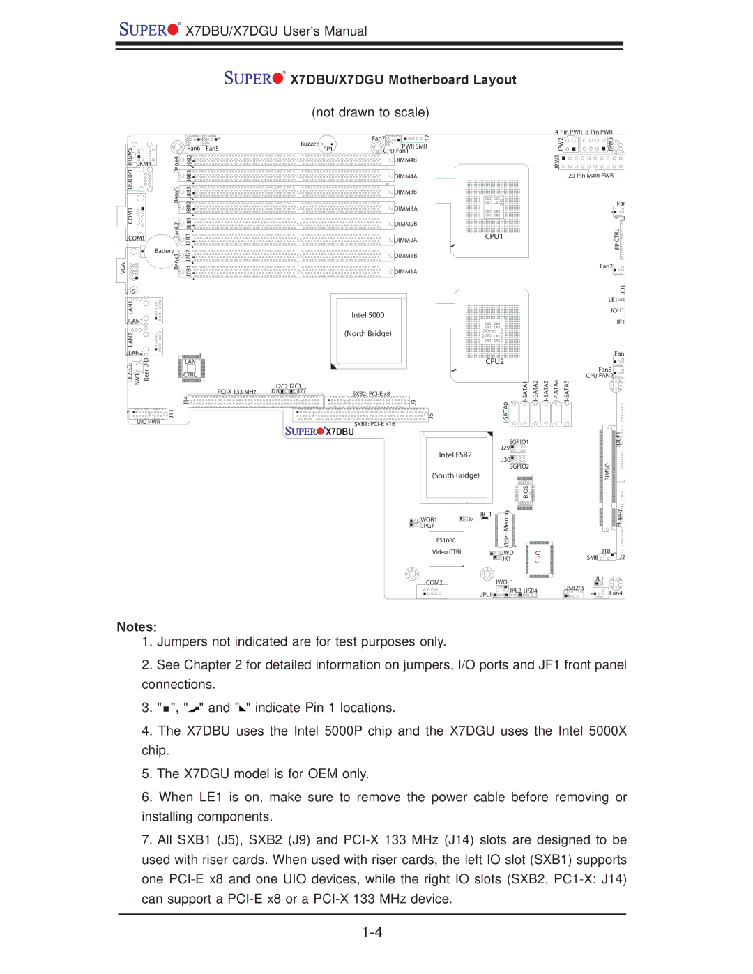
 X7DBU/X7DGU Motherboard Layout
(not drawn to scale)
|
|
|
|
|
| Buzzer |
| Fan7 | J17 |
|
|
|
|
|
| JPW2 |
| JPW3 |
|
|
|
|
|
|
| CPU Fan1 |
|
|
|
|
|
|
|
| |||
KB/MS0/1 USBCOM1 |
|
| Fan6 | Fan5 |
|
| SP1 | PWR SMB |
|
|
|
|
|
|
|
|
| |
| Bank4 Bank3Bank2 |
|
|
|
|
|
|
|
|
|
| JPW1 |
|
| ||||
| J9B1J9B2 J8B2J8B1J8B3 |
|
|
|
| DIMM4B |
|
|
|
|
|
|
|
|
| |||
JKM1 |
|
|
|
|
|
|
|
|
|
|
|
|
|
|
|
|
| |
|
|
|
|
|
|
|
| DIMM4A |
|
|
|
|
|
|
|
| ||
|
|
|
|
|
|
|
| DIMM3B |
|
|
|
|
|
|
|
|
|
|
|
|
|
|
|
|
|
| DIMM3A |
|
|
|
|
|
|
|
|
| Fan |
|
|
|
|
|
|
|
|
|
|
|
|
|
|
|
|
|
| |
|
|
|
|
|
|
|
| DIMM2B |
|
|
|
|
|
|
|
|
| JF |
|
|
| J7B3J7B2 |
|
|
|
|
|
|
|
|
|
|
|
|
| CTRLFP | |
JCOM1 |
|
|
|
|
| DIMM2A |
|
| CPU1 |
|
|
|
|
| ||||
|
|
|
|
|
|
|
|
|
|
|
|
|
| |||||
|
|
|
|
|
|
|
|
|
|
|
|
|
|
|
|
|
| |
| Battery |
|
|
|
|
| DIMM1B |
|
|
|
|
|
|
|
|
|
| |
VGA |
| Bank1 | J7B1 |
|
|
|
|
|
|
|
|
|
|
|
|
|
| |
|
|
|
|
| DIMM1A |
|
|
|
|
|
|
|
|
| Fan2 | |||
|
|
|
|
|
|
|
|
|
|
|
|
|
|
|
|
|
| |
J15 |
|
|
|
|
|
|
|
|
|
|
|
|
|
|
|
|
| JD1 |
LAN1 |
|
|
|
|
|
|
|
|
|
|
|
|
|
|
|
|
| LE1 |
|
|
|
|
|
|
| Intel 5000 |
|
|
|
|
|
|
|
|
| JOH1 | |
JLAN1 |
|
|
|
|
|
|
|
|
|
|
|
|
|
|
|
| JP1 | |
|
|
|
|
|
|
|
|
|
|
|
|
|
|
|
|
| ||
LAN2 |
|
|
|
|
|
|
| (North Bridge) |
|
|
|
|
|
|
|
|
|
|
|
|
|
|
|
|
|
|
|
|
|
|
|
|
|
|
|
| |
JLAN2 | UID |
|
|
|
|
|
|
|
|
|
|
|
|
|
|
|
| Fan |
|
| LAN |
|
|
|
|
|
|
| CPU2 |
|
|
|
|
|
| ||
|
|
|
|
|
|
|
|
|
|
|
|
|
|
|
| |||
SW1 | Rear |
| CTRL |
|
|
|
|
|
|
|
|
|
|
|
|
|
| Fan8 |
LE2 UIO PWR | J11 |
|
|
|
| J9 | J5 |
|
| CPU FAN2 | ||||||||
J14 | I2C2 | I2C1 |
|
|
|
| ||||||||||||
|
|
|
| J28 | J27 |
| SXB2: |
|
|
|
|
|
|
|
|
|
| |
|
|
|
|
|
|
|
|
|
|
|
|
|
|
|
|
|
| |
|
|
|
|
|
|
|
| SXB1: |
|
|
|
|
|
|
|
|
|
|
|
|
|
|
|
|
| X7DBU |
|
|
|
|
|
|
|
|
| IDE#1 | |
|
|
|
|
|
|
|
|
|
|
|
| SGPIO1 |
|
|
|
| ||
|
|
|
|
|
|
|
|
| Intel ESB2 |
| J29 |
|
|
|
|
|
| |
|
|
|
|
|
|
|
|
|
| J30 |
|
|
|
|
|
| ||
|
|
|
|
|
|
|
|
|
|
|
|
|
|
|
|
| SIMSO | |
|
|
|
|
|
|
|
|
|
|
|
| SGPIO2 |
|
|
|
| ||
|
|
|
|
|
|
|
|
| (South Bridge) |
|
|
|
|
|
|
| ||
|
|
|
|
|
|
|
|
|
|
|
| Memory | BIOS |
|
|
|
| Floppy |
|
|
|
|
|
|
|
|
| JWOR1 | J7 | JBT1 |
|
|
|
|
| ||
|
|
|
|
|
|
|
|
|
|
|
|
|
|
|
|
| ||
|
|
|
|
|
|
|
|
| JPG1 |
|
| Video |
|
|
|
|
|
|
|
|
|
|
|
|
|
|
| ES1000 |
|
|
|
|
|
|
|
| |
|
|
|
|
|
|
|
|
|
|
|
|
|
|
|
|
|
| |
|
|
|
|
|
|
|
|
| Video CTRL |
|
| JWD |
| I/O |
|
| SMB | J18 |
|
|
|
|
|
|
|
|
|
|
|
| JK1 |
|
|
| J2 | ||
|
|
|
|
|
|
|
|
|
|
|
|
| S |
|
|
|
| |
|
|
|
|
|
|
|
|
|
|
|
|
|
|
|
|
|
| |
|
|
|
|
|
|
|
|
| COM2 |
|
| JWOL1 |
|
|
|
| JL1 | |
|
|
|
|
|
|
|
|
|
|
|
|
|
|
| USB2/3 |
| ||
|
|
|
|
|
|
|
|
|
|
| JPL1 | JPL2 USB4 |
|
| Fan4 | |||
|
|
|
|
|
|
|
|
|
|
|
|
|
| |||||
|
|
|
|
|
|
|
|
|
|
|
|
|
|
|
|
| ||
Notes:
1.Jumpers not indicated are for test purposes only.
2.See Chapter 2 for detailed information on jumpers, I/O ports and JF1 front panel connections.
3." ![]() ", "
", "![]() " and "
" and "![]() " indicate Pin 1 locations.
" indicate Pin 1 locations.
4.The X7DBU uses the Intel 5000P chip and the X7DGU uses the Intel 5000X chip.
5.The X7DGU model is for OEM only.
6.When LE1 is on, make sure to remove the power cable before removing or installing components.
7.All SXB1 (J5), SXB2 (J9) and
can support a