Chapter 2: Installation
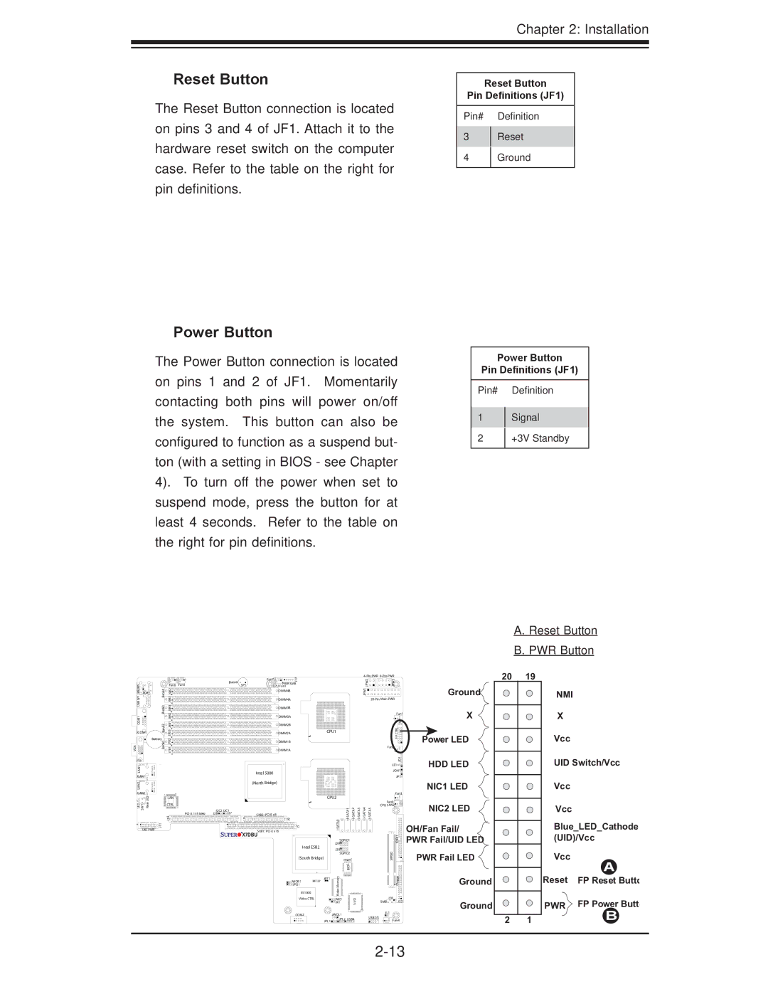
Reset Button
The Reset Button connection is located on pins 3 and 4 of JF1. Attach it to the hardware reset switch on the computer case. Refer to the table on the right for pin definitions.
Power Button
The Power Button connection is located on pins 1 and 2 of JF1. Momentarily contacting both pins will power on/off the system. This button can also be configured to function as a suspend but- ton (with a setting in BIOS - see Chapter 4). To turn off the power when set to suspend mode, press the button for at least 4 seconds. Refer to the table on the right for pin definitions.
Reset Button
Pin Definitions (JF1)
Pin# Definition
3Reset
4Ground
Power Button
Pin Definitions (JF1)
Pin# Definition
1Signal
2+3V Standby
A. Reset Button
B. PWR Button
|
|
|
|
| Fan7 | 71 |
|
|
|
|
| Buzzer |
| J |
|
|
| Fan6 | Fan5 | SP1 |
| PWR SMB |
|
|
| CPU Fan1 |
| ||||
JKM1 |
|
|
|
|
| DIMM4B |
|
KB/MS0/1USB COM1 | Bank3Bank4 | J9B1J9B2 J8B2J8B3 J8B1 |
|
|
| DIMM4A |
|
|
|
| DIMM3B |
| |||
|
|
| DIMM3A |
| |||
|
|
| DIMM2B |
| |||
JCOM1 | Bank2 | J7B3 |
|
|
| DIMM2A | CPU1 |
|
|
|
|
|
| ||
| Battery | J7B2 |
|
|
| DIMM1B |
|
| Bank1 |
|
|
|
| ||
VGA |
|
|
|
|
| ||
J7B1 |
|
|
| DIMM1A |
| ||
| 20 | 19 | ||
2W PJ | 3W PJ |
|
|
|
1W PJ |
|
| Ground | NMI |
|
|
| ||
|
| Fan1 | X | X |
|
| JF1 |
|
|
|
| LRT C |
|
|
FP | Power LED | Vcc |
Fan2
J15 |
|
|
|
|
|
|
|
|
|
|
|
LAN1 |
|
|
|
| Intel 5000 |
|
|
|
|
| |
JLAN1 |
|
|
|
|
|
|
|
|
| ||
|
|
|
|
|
|
|
|
|
|
| |
LAN2 |
|
|
|
| (North Bridge) |
|
|
|
|
| |
|
|
|
|
|
|
|
|
|
|
| |
JLAN2 |
|
|
|
|
|
|
|
|
|
|
|
| UID | LAN |
|
|
|
| CPU2 |
|
|
| |
LE2 SW1 | Rear | CTRL |
|
|
|
|
|
|
|
|
|
| I2C2 | I2C1 |
|
|
|
| 1AT AS- I | 2AT AS- I | 3AT AS- I | ||
J28 | J27 | SXB2: |
|
| |||||||
J14 |
|
|
| 9J |
| 0 | |||||
UIO PWR | J11 |
|
|
| 5J |
| ATSA |
|
|
| |
|
|
|
|
| X7DBU | SXB1: |
|
|
|
|
|
|
|
|
|
|
|
|
|
|
|
| |
|
|
|
|
|
|
|
|
| SGPIO1 |
|
|
|
|
|
|
|
|
| Intel ESB2 | J29 |
|
| |
|
|
|
|
|
|
| J30 |
|
| ||
|
|
|
|
|
|
|
|
|
| ||
|
|
|
|
|
|
|
|
| SGPIO2 |
|
|
|
|
|
|
|
| (South Bridge) |
|
|
|
| |
|
|
|
|
|
|
|
|
| SBIO |
|
|
|
|
|
|
|
|
| JBT1 | ry |
|
|
|
|
|
|
|
|
| JWOR1 | J7 | Memo |
|
|
|
|
|
|
|
|
| JPG1 |
|
|
|
| |
|
|
|
|
|
| ES1000 | Video |
|
|
| |
|
|
|
|
|
|
|
|
|
|
| |
1DJ | HDD LED |
LE1 | |
JOH1 |
|
JP1 |
|
| NIC1 LED |
Fan3 |
|
Fan8 |
|
CPU FAN2 | NIC2 LED |
| |
| OH/Fan Fail/ |
1E# ID | PWR Fail/UID LED |
SIMSO | PWR Fail LED |
Floppy | Ground |
UID Switch/Vcc
Vcc
Vcc
Blue_LED_Cathode (UID)/Vcc
Vcc
A
Reset FP Reset Butto
Video CTRL | JWD | O |
| JK1 | I/ |
|
| S |
COM2 | JWOL1 |
|
| JPL2 | USB4 |
| JPL1 |
|
| J18 |
|
|
|
SMB | J22 |
| PWR | FP Power Butt |
| Ground |
| ||
JL1 |
|
| B | |
USB2/3 | Fan4 | 2 | 1 | |
| ||||