MSP430x11x1
Description
Tssop
Pulldown resistor of 30 k Ω is needed on F11x1
Functional block diagram
Available Options Packaged Devices
PIN Sowb PIN Tssop
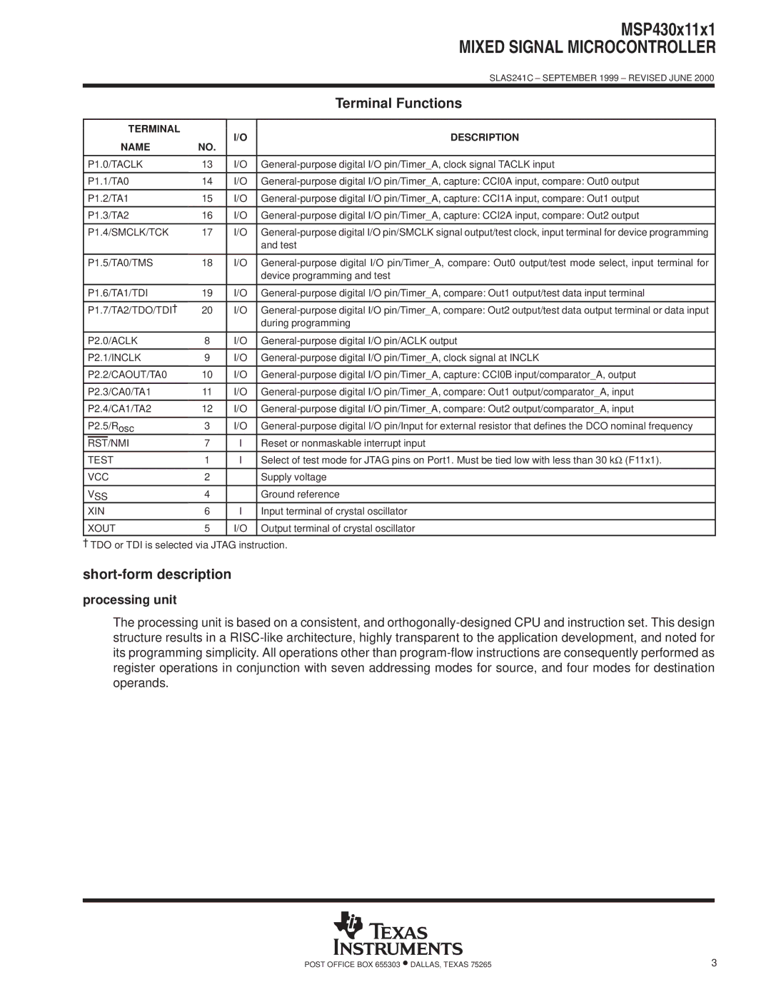
Terminal Description Name
Terminal Functions
Short-form description
Processing unit
Instruction Word Formats
Address Mode Descriptions
CPU
Instruction set
Operation modes and interrupts
Low-power consumption capabilities
SCG1 SCG0
Status register R2
SCG1
SCG0
CCIFG1, CCIFG2, Taifg
Interrupt vector addresses
Caifg
Wdtifg
Nmiifg
Special function registers
Wdtifg
Ofifg
Boot ROM containing bootstrap loader
Functions of the bootstrap loader
Memory organization
VCC RST/NMI PIN Test PIN
Features of the bootstrap loader are
Hardware resources used for serial input/output
WDT
Internal
Bootstrap loader Starts
VCC
Test
Flash memory control register FCTL1
Flash memory
Flash memory, timing generator, control register FCTL2
Erase 0128h, bit1, Erase a segment
WRT
Aclk
Flash memory control register FCTL3
FN0±FN5
SSEL0, SSEL1
Wait
Busy
Keyv
Accvifg
Flash memory, interrupt and security key violation
Lock
Emex
Nmirs
Accv
PUC
POR
Oscillator and system clock
Peripherals
Digital I/O
Clock Signals
TimerA Three capture/compare registers
Watchdog timer
TimerA, MSP430x11x1 Configuration
TimerA 3 capture/compare registers
ComparatorA
CATCTL2.7
Caout
CAF
CACTL2.4
CACTL2
Slope a/d conversion
CACTL1
Caex Caon Caies Caifg Rsel REF1 REF0
Peripherals with Word Access
Peripherals with Byte Access
Peripheral file map
Absolute maximum ratings²
Recommended operating conditions
MIN NOM MAX Units
Frequency vs Supply Voltage
MSP430x11x1 Devices
ILPM3
Parameter Test Conditions MIN TYP MAX Unit
IAM
ILPM2
Leakage current
Outputs Port 1 to P2 P1.0 to P1.7, P2.0 to P2.5
Port P1, P2 P1.x to P2.x
Internal signals TAx, Smclk at TimerA
Inputs Px.x, TAx
Parameter Test Conditions VCC MIN TYP MAX Unit
ComparatorA see Note
Outputs P1.x, P2.x, TAx
VRefVT vs Temperature, VCC = 2.2 V, C1121
VRefVT vs Temperature, VCC = 3 V, C1121
CAF Caon
PUC/POR
Parameter MIN NOM MAX Unit
RAM
DCO Steps
DCO
Variance Max
Dcoclk
Principle characteristics of the DCO
Wake-up from lower power modes LPMx
JTAG/programming
Input/output schematic
Port P1, P1.0 to P1.3, input/output with Schmitt-trigger
GND
P1IFG.5 P1IES.5
P1DIR.4 P1OUT.4 Smclk
P1IFG.4 P1IES.4
P1DIR.5 P1OUT.5
CAPD.X
Port P2, P2.0 to P2.2, input/output with Schmitt-trigger
P2DIR.4 P2OUT.4
Port P2, P2.3 to P2.4, input/output with Schmitt-trigger
P2DIR.3 P2OUT.3
P2IFG.3 P1IES.3
P2IRQ.5
P2SEL.5 VCC
P2DIR.5
P2OUT.5
Port P2, unbonded bits P2.6 and P2.7
PIN Shown
Pins DIM MAX
DW R-PDSO-G
Plastic SMALL-OUTLINE Package
15 NOM Gage Plane Seating Plane 20 MAX
Pins Shown
Pins DIM MAX MIN
PW R-PDSO-G Plastic SMALL-OUTLINE Package
Important Notice