www.ti.com | Peripheral Architecture |
•Following a write to the two
At the end of the initialization sequence, the DDR2 memory controller performs an
When the initialization section is started automatically after a hard or soft reset, commands and data stored in the DDR2 memory controller FIFOs are lost. However, when the initialization sequence is initiated by a write to the two
2.11.1DDR2 SDRAM Device Mode Register Configuration Values
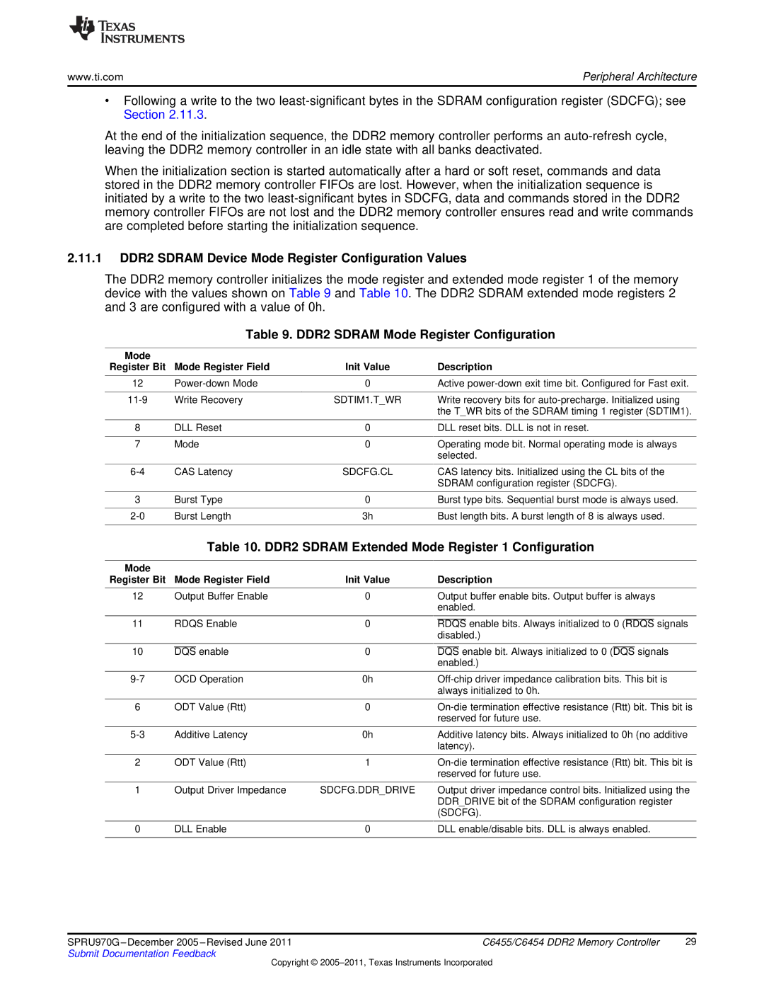
The DDR2 memory controller initializes the mode register and extended mode register 1 of the memory device with the values shown on Table 9 and Table 10. The DDR2 SDRAM extended mode registers 2 and 3 are configured with a value of 0h.
Table 9. DDR2 SDRAM Mode Register Configuration
Mode |
|
|
|
Register Bit | Mode Register Field | Init Value | Description |
|
|
|
|
12 | 0 | Active | |
|
|
|
|
Write Recovery | SDTIM1.T_WR | Write recovery bits for | |
|
|
| the T_WR bits of the SDRAM timing 1 register (SDTIM1). |
|
|
|
|
8 | DLL Reset | 0 | DLL reset bits. DLL is not in reset. |
|
|
|
|
7 | Mode | 0 | Operating mode bit. Normal operating mode is always |
|
|
| selected. |
|
|
|
|
CAS Latency | SDCFG.CL | CAS latency bits. Initialized using the CL bits of the | |
|
|
| SDRAM configuration register (SDCFG). |
|
|
|
|
3 | Burst Type | 0 | Burst type bits. Sequential burst mode is always used. |
|
|
|
|
Burst Length | 3h | Bust length bits. A burst length of 8 is always used. | |
|
|
|
|
Table 10. DDR2 SDRAM Extended Mode Register 1 Configuration
Mode |
|
|
|
|
|
|
|
|
|
|
|
Register Bit | Mode Register Field | Init Value |
| Description | |||||||
|
|
|
|
| |||||||
12 | Output Buffer Enable | 0 |
| Output buffer enable bits. Output buffer is always | |||||||
|
|
|
|
| enabled. | ||||||
|
|
|
|
|
|
|
| ||||
11 | RDQS Enable | 0 |
|
|
| enable bits. Always initialized to 0 |
|
| signals | ||
| RDQS | (RDQS | |||||||||
|
|
|
|
| disabled.) | ||||||
|
|
|
|
|
|
|
|
|
|
|
|
10 |
| enable | 0 |
|
| enable bit. Always initialized to 0 |
|
| signals | ||
DQS |
| DQS | (DQS | ||||||||
|
|
|
|
| enabled.) | ||||||
|
|
|
|
|
|
|
|
|
|
|
|
OCD Operation | 0h |
| |||||||||
|
|
|
|
| always initialized to 0h. | ||||||
|
|
|
|
|
|
|
|
|
|
|
|
6 | ODT Value (Rtt) | 0 |
| ||||||||
|
|
|
|
| reserved for future use. | ||||||
|
|
|
|
|
|
|
|
|
|
|
|
Additive Latency | 0h |
| Additive latency bits. Always initialized to 0h (no additive | ||||||||
|
|
|
|
| latency). | ||||||
|
|
|
|
|
|
|
|
|
|
|
|
2 | ODT Value (Rtt) | 1 |
| ||||||||
|
|
|
|
| reserved for future use. | ||||||
|
|
|
|
|
|
|
|
|
|
|
|
1 | Output Driver Impedance | SDCFG.DDR_DRIVE |
| Output driver impedance control bits. Initialized using the | |||||||
|
|
|
|
| DDR_DRIVE bit of the SDRAM configuration register | ||||||
|
|
|
|
| (SDCFG). | ||||||
|
|
|
|
|
|
|
|
|
|
|
|
0 | DLL Enable | 0 |
| DLL enable/disable bits. DLL is always enabled. | |||||||
|
|
|
|
|
|
|
|
|
|
|
|
SPRU970G – December 2005 – Revised June 2011 | C6455/C6454 DDR2 Memory Controller | 29 |
Submit Documentation Feedback |
|
|
Copyright ©