Peripheral Architecturewww.ti.com
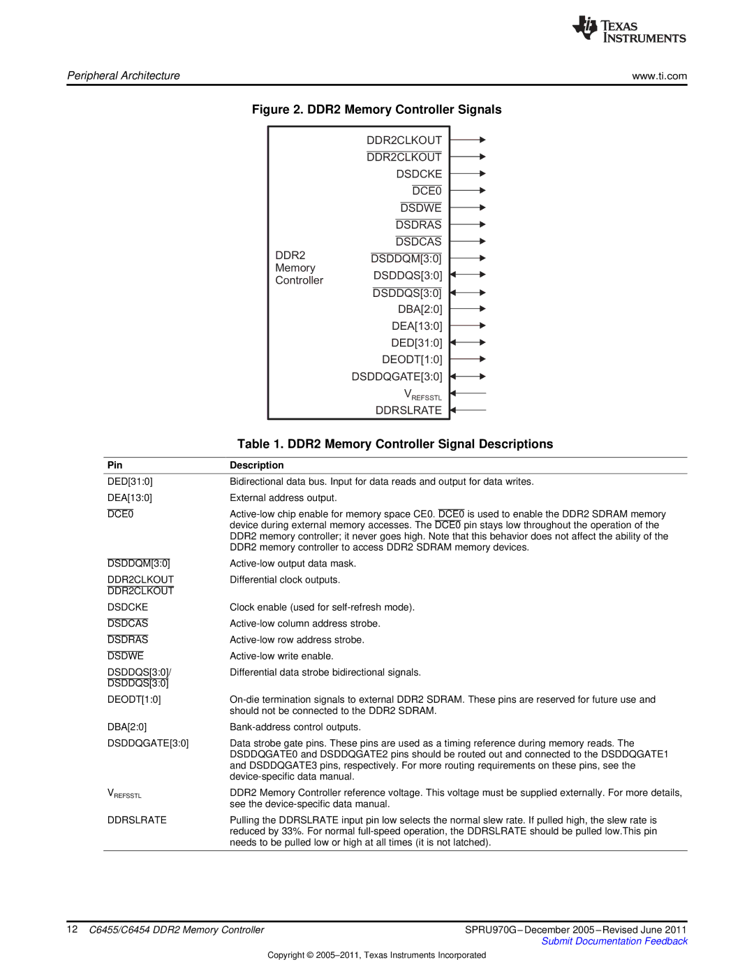
Figure 2. DDR2 Memory Controller Signals
|
|
|
|
|
|
|
|
|
| DDR2CLKOUT |
|
|
|
|
|
| |||||||||
|
|
|
|
|
|
|
|
|
|
|
|
|
| ||||||||||||
|
|
|
|
|
|
|
|
|
|
|
|
|
|
|
|
|
|
|
|
|
|
|
|
|
|
|
|
|
|
|
|
|
|
|
| DDR2CLKOUT |
|
|
|
|
|
| |||||||||
|
|
|
|
|
|
|
|
|
|
|
|
|
| ||||||||||||
|
|
|
|
|
|
|
|
|
|
|
|
| DSDCKE |
|
|
|
|
|
| ||||||
|
|
|
|
|
|
|
|
|
|
|
|
|
| ||||||||||||
|
|
|
|
|
|
|
|
|
|
|
|
|
|
|
|
|
|
|
|
|
|
|
| ||
|
|
|
|
|
|
|
|
|
|
|
|
|
|
| DCE0 |
|
|
|
|
|
| ||||
|
|
|
|
|
|
|
|
|
|
|
|
|
|
|
|
|
|
| |||||||
|
|
|
|
|
|
|
|
|
|
|
|
|
|
|
|
|
|
|
|
|
|
|
| ||
|
|
|
|
|
|
|
|
|
|
|
|
|
| DSDWE |
|
|
|
|
|
| |||||
|
|
|
|
|
|
|
|
|
|
|
|
|
|
|
|
|
| ||||||||
|
|
|
|
|
|
|
|
|
|
|
|
|
|
|
|
|
|
|
|
|
|
| |||
|
|
|
|
|
|
|
|
|
|
|
|
| DSDRAS |
|
|
|
|
|
| ||||||
|
|
|
|
|
|
|
|
|
|
|
|
|
|
|
|
| |||||||||
|
|
|
|
|
|
|
|
|
|
|
|
|
|
|
|
|
|
|
|
|
| ||||
|
|
|
|
|
|
|
|
| DDR2 |
|
|
| DSDCAS |
|
|
|
|
|
| ||||||
|
|
|
|
|
|
|
|
|
|
|
|
|
|
|
| ||||||||||
|
|
|
|
|
|
|
|
|
|
|
|
|
|
|
|
|
|
|
|
|
|
|
|
| |
|
|
|
|
|
|
|
|
| DSDDQM[3:0] |
|
|
|
|
|
| ||||||||||
|
|
|
|
|
|
|
|
|
|
|
|
|
|
| |||||||||||
|
|
|
|
|
|
|
|
| Memory |
|
|
|
| ||||||||||||
|
|
|
|
|
|
|
|
|
|
| DSDDQS[3:0] |
|
|
|
|
|
| ||||||||
|
|
|
|
|
|
|
|
| Controller |
|
|
|
|
|
|
|
| ||||||||
|
|
|
|
|
|
|
|
|
|
|
|
|
|
|
|
|
|
|
|
|
|
|
|
| |
|
|
|
|
|
|
|
|
|
|
|
| DSDDQS[3:0] |
|
|
|
|
| ||||||||
|
|
|
|
|
|
|
|
|
|
|
|
|
|
| |||||||||||
|
|
|
|
|
|
|
|
|
|
|
|
| DBA[2:0] |
|
|
|
|
|
| ||||||
|
|
|
|
|
|
|
|
|
|
|
|
|
|
|
|
| |||||||||
|
|
|
|
|
|
|
|
|
|
|
| DEA[13:0] |
|
|
|
|
| ||||||||
|
|
|
|
|
|
|
|
|
|
|
|
|
| ||||||||||||
|
|
|
|
|
|
|
|
|
|
|
| DED[31:0] |
|
|
|
|
|
| |||||||
|
|
|
|
|
|
|
|
|
|
|
|
|
| ||||||||||||
|
|
|
|
|
|
|
|
|
|
|
| DEODT[1:0] |
|
|
|
| |||||||||
|
|
|
|
|
|
|
|
|
|
|
|
|
|
| |||||||||||
|
|
|
|
|
|
|
|
| DSDDQGATE[3:0] |
|
|
|
|
| |||||||||||
|
|
|
|
|
|
|
|
|
|
| |||||||||||||||
|
|
|
|
|
|
|
|
|
|
|
|
|
| VREFSSTL |
|
|
|
|
| ||||||
|
|
|
|
|
|
|
|
|
|
|
|
|
|
|
|
| |||||||||
|
|
|
|
|
|
|
|
|
|
|
| DDRSLRATE |
|
|
| ||||||||||
|
|
|
|
|
|
|
|
|
|
|
|
|
|
|
|
|
| ||||||||
|
|
|
|
|
|
|
| Table 1. DDR2 Memory Controller Signal Descriptions | |||||||||||||||||
|
|
|
|
|
|
|
|
|
|
|
|
|
|
|
|
|
|
| |||||||
| Pin | Description |
|
|
|
|
|
|
|
|
|
|
|
|
|
|
|
| |||||||
|
|
| |||||||||||||||||||||||
| DED[31:0] | Bidirectional data bus. Input for data reads and output for data writes. | |||||||||||||||||||||||
| DEA[13:0] | External address output. |
|
|
|
|
|
|
|
|
|
|
|
|
|
|
|
| |||||||
|
|
|
| is used to enable the DDR2 SDRAM memory | |||||||||||||||||||||
| DCE0 | DCE0 | |||||||||||||||||||||||
|
|
|
|
|
|
|
| device during external memory accesses. The | DCE0 | pin stays low throughout the operation of the | |||||||||||||||
|
|
|
|
|
|
|
| DDR2 memory controller; it never goes high. Note that this behavior does not affect the ability of the | |||||||||||||||||
|
|
|
|
|
|
|
| DDR2 memory controller to access DDR2 SDRAM memory devices. | |||||||||||||||||
|
|
|
|
|
|
|
|
|
|
|
|
|
|
|
|
|
|
|
| ||||||
| DSDDQM[3:0] |
|
|
|
|
|
|
|
|
|
|
|
|
|
|
|
| ||||||||
| DDR2CLKOUT | Differential clock outputs. |
|
|
|
|
|
|
|
|
|
|
|
|
|
|
|
| |||||||
| DDR2CLKOUT |
|
|
|
|
|
|
|
|
|
|
|
|
|
|
|
|
|
|
| |||||
| DSDCKE | Clock enable (used for | |||||||||||||||||||||||
|
|
|
|
|
| ||||||||||||||||||||
| DSDCAS | ||||||||||||||||||||||||
|
|
|
|
|
|
|
|
|
|
|
|
|
|
|
|
|
|
|
|
|
| ||||
| DSDRAS |
|
|
|
|
|
|
|
|
|
|
|
|
|
|
|
| ||||||||
|
|
|
|
|
|
|
|
|
|
|
|
|
|
|
|
|
|
|
|
|
|
| |||
| DSDWE |
|
|
|
|
|
|
|
|
|
|
|
|
|
|
|
| ||||||||
| DSDDQS[3:0]/ | Differential data strobe bidirectional signals. | |||||||||||||||||||||||
| DSDDQS[3:0] |
|
|
|
|
|
|
|
|
|
|
|
|
|
|
|
|
|
|
|
|
| |||
| DEODT[1:0] | ||||||||||||||||||||||||
|
|
|
|
|
|
|
| should not be connected to the DDR2 SDRAM. | |||||||||||||||||
| DBA[2:0] |
|
|
|
|
|
|
|
|
|
|
|
|
|
|
|
| ||||||||
| DSDDQGATE[3:0] | Data strobe gate pins. These pins are used as a timing reference during memory reads. The | |||||||||||||||||||||||
|
|
|
|
|
|
|
| DSDDQGATE0 and DSDDQGATE2 pins should be routed out and connected to the DSDDQGATE1 | |||||||||||||||||
|
|
|
|
|
|
|
| and DSDDQGATE3 pins, respectively. For more routing requirements on these pins, see the | |||||||||||||||||
|
|
|
|
|
|
|
|
|
|
|
|
|
|
|
|
|
|
|
|
|
|
|
| ||
| VREFSSTL | DDR2 Memory Controller reference voltage. This voltage must be supplied externally. For more details, | |||||||||||||||||||||||
|
|
|
|
|
|
|
| see the | |||||||||||||||||
| DDRSLRATE | Pulling the DDRSLRATE input pin low selects the normal slew rate. If pulled high, the slew rate is | |||||||||||||||||||||||
|
|
|
|
|
|
|
| reduced by 33%. For normal | |||||||||||||||||
|
|
|
|
|
|
|
| needs to be pulled low or high at all times (it is not latched). | |||||||||||||||||
|
|
|
|
|
|
|
|
|
|
|
|
|
|
|
|
|
|
|
|
|
|
|
|
|
|
12 C6455/C6454 DDR2 Memory Controller | SPRU970G – December 2005 – Revised June 2011 |
| Submit Documentation Feedback |
Copyright ©