www.ti.com | DDR2 Memory Controller Registers |
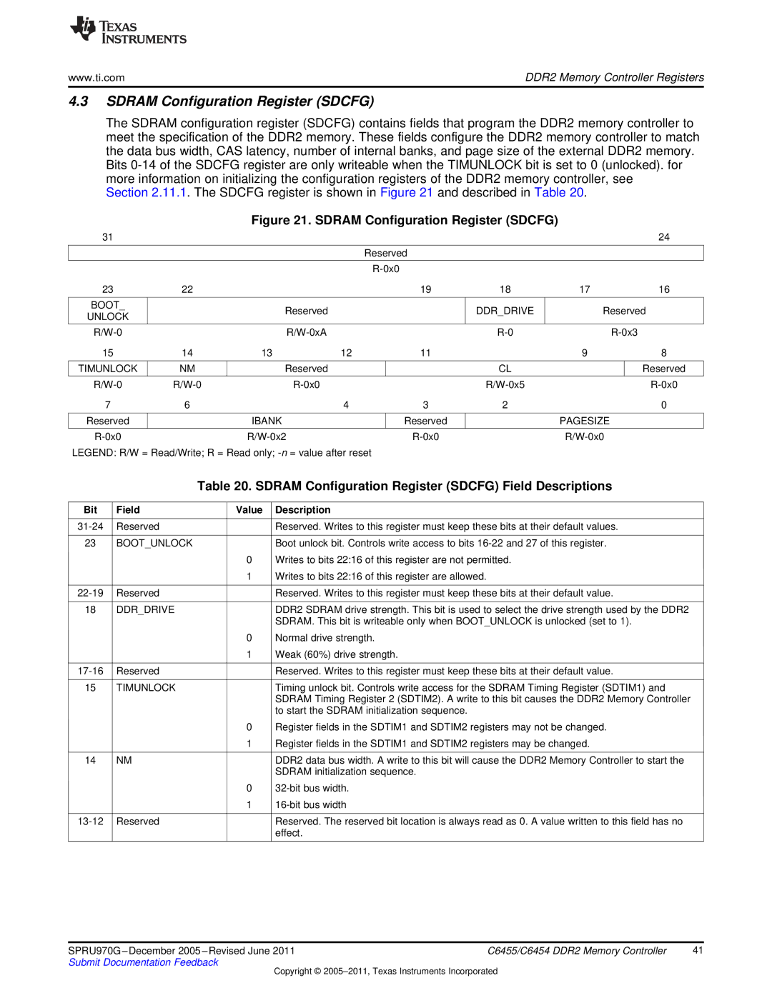
4.3SDRAM Configuration Register (SDCFG)
The SDRAM configuration register (SDCFG) contains fields that program the DDR2 memory controller to meet the specification of the DDR2 memory. These fields configure the DDR2 memory controller to match the data bus width, CAS latency, number of internal banks, and page size of the external DDR2 memory. Bits
Section 2.11.1. The SDCFG register is shown in Figure 21 and described in Table 20.
Figure 21. SDRAM Configuration Register (SDCFG)
31 |
|
|
|
|
|
|
| 24 | |
|
|
|
| Reserved |
|
|
|
| |
|
|
|
|
|
|
|
| ||
23 | 22 |
|
| 19 | 18 | 17 | 16 | ||
|
|
|
|
|
|
|
|
|
|
BOOT_ |
| Reserved |
|
|
| DDR_DRIVE | Reserved | ||
UNLOCK |
|
|
|
| |||||
|
|
|
|
|
|
|
|
| |
|
|
|
|
| |||||
15 | 14 | 13 | 12 | 11 |
| 9 | 8 | ||
|
|
|
|
|
|
|
|
|
|
TIMUNLOCK | NM | Reserved |
|
|
| CL |
|
| Reserved |
|
|
|
|
|
|
|
|
|
|
|
|
|
|
| |||||
7 | 6 |
| 4 | 3 | 2 |
| 0 | ||
|
|
|
|
|
|
|
|
|
|
Reserved |
| IBANK |
|
| Reserved |
| PAGESIZE |
|
|
|
|
|
|
|
|
|
|
|
|
|
|
|
|
|
| ||||
LEGEND: R/W = Read/Write; R = Read only;
Table 20. SDRAM Configuration Register (SDCFG) Field Descriptions
Bit | Field | Value | Description |
|
|
|
|
Reserved |
| Reserved. Writes to this register must keep these bits at their default values. | |
|
|
|
|
23 | BOOT_UNLOCK |
| Boot unlock bit. Controls write access to bits |
|
| 0 | Writes to bits 22:16 of this register are not permitted. |
|
| 1 | Writes to bits 22:16 of this register are allowed. |
|
|
|
|
Reserved |
| Reserved. Writes to this register must keep these bits at their default value. | |
|
|
|
|
18 | DDR_DRIVE |
| DDR2 SDRAM drive strength. This bit is used to select the drive strength used by the DDR2 |
|
|
| SDRAM. This bit is writeable only when BOOT_UNLOCK is unlocked (set to 1). |
|
| 0 | Normal drive strength. |
|
| 1 | Weak (60%) drive strength. |
|
|
|
|
Reserved |
| Reserved. Writes to this register must keep these bits at their default value. | |
|
|
|
|
15 | TIMUNLOCK |
| Timing unlock bit. Controls write access for the SDRAM Timing Register (SDTIM1) and |
|
|
| SDRAM Timing Register 2 (SDTIM2). A write to this bit causes the DDR2 Memory Controller |
|
|
| to start the SDRAM initialization sequence. |
|
| 0 | Register fields in the SDTIM1 and SDTIM2 registers may not be changed. |
|
| 1 | Register fields in the SDTIM1 and SDTIM2 registers may be changed. |
|
|
|
|
14 | NM |
| DDR2 data bus width. A write to this bit will cause the DDR2 Memory Controller to start the |
|
|
| SDRAM initialization sequence. |
|
| 0 | |
|
| 1 | |
|
|
|
|
Reserved |
| Reserved. The reserved bit location is always read as 0. A value written to this field has no | |
|
|
| effect. |
|
|
|
|
SPRU970G – December 2005 – Revised June 2011 | C6455/C6454 DDR2 Memory Controller | 41 |
Submit Documentation Feedback |
|
|
Copyright ©