Using the DDR2 Memory Controller | www.ti.com |
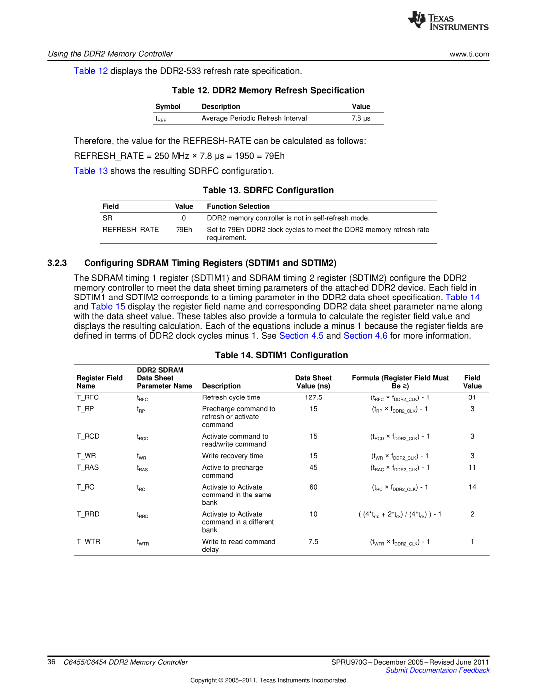
Table 12 displays the
Table 12. DDR2 Memory Refresh Specification
Symbol | Description | Value |
tREF | Average Periodic Refresh Interval | 7.8 μs |
Therefore, the value for the
REFRESH_RATE = 250 MHz × 7.8 μs = 1950 = 79Eh
Table 13 shows the resulting SDRFC configuration.
|
| Table 13. SDRFC Configuration | |
|
|
|
|
Field | Value |
| Function Selection |
|
|
|
|
SR | 0 |
| DDR2 memory controller is not in |
REFRESH_RATE | 79Eh |
| Set to 79Eh DDR2 clock cycles to meet the DDR2 memory refresh rate |
|
|
| requirement. |
|
|
|
|
3.2.3Configuring SDRAM Timing Registers (SDTIM1 and SDTIM2)
The SDRAM timing 1 register (SDTIM1) and SDRAM timing 2 register (SDTIM2) configure the DDR2 memory controller to meet the data sheet timing parameters of the attached DDR2 device. Each field in SDTIM1 and SDTIM2 corresponds to a timing parameter in the DDR2 data sheet specification. Table 14 and Table 15 display the register field name and corresponding DDR2 data sheet parameter name along with the data sheet value. These tables also provide a formula to calculate the register field value and displays the resulting calculation. Each of the equations include a minus 1 because the register fields are defined in terms of DDR2 clock cycles minus 1. See Section 4.5 and Section 4.6 for more information.
Table 14. SDTIM1 Configuration
| DDR2 SDRAM |
|
|
|
|
Register Field | Data Sheet |
| Data Sheet | Formula (Register Field Must | Field |
Name | Parameter Name | Description | Value (ns) | Be ≥) | Value |
T_RFC | tRFC | Refresh cycle time | 127.5 | (tRFC × fDDR2_CLK) - 1 | 31 |
T_RP | tRP | Precharge command to | 15 | (tRP × fDDR2_CLK) - 1 | 3 |
|
| refresh or activate |
|
|
|
|
| command |
|
|
|
T_RCD | tRCD | Activate command to | 15 | (tRCD × fDDR2_CLK) - 1 | 3 |
|
| read/write command |
|
|
|
T_WR | tWR | Write recovery time | 15 | (tWR × fDDR2_CLK) - 1 | 3 |
T_RAS | tRAS | Active to precharge | 45 | (tRAC × fDDR2_CLK) - 1 | 11 |
|
| command |
|
|
|
T_RC | tRC | Activate to Activate | 60 | (tRC × fDDR2_CLK) - 1 | 14 |
|
| command in the same |
|
|
|
|
| bank |
|
|
|
T_RRD | tRRD | Activate to Activate | 10 | ( (4*trrd + 2*tck) / (4*tck) ) - 1 | 2 |
|
| command in a different |
|
|
|
|
| bank |
|
|
|
T_WTR | tWTR | Write to read command | 7.5 | (tWTR × fDDR2_CLK) - 1 | 1 |
|
| delay |
|
|
|
|
|
|
|
|
|
36 C6455/C6454 DDR2 Memory Controller | SPRU970G – December 2005 – Revised June 2011 |
| Submit Documentation Feedback |
Copyright ©