Peripheral Architecture | www.ti.com |
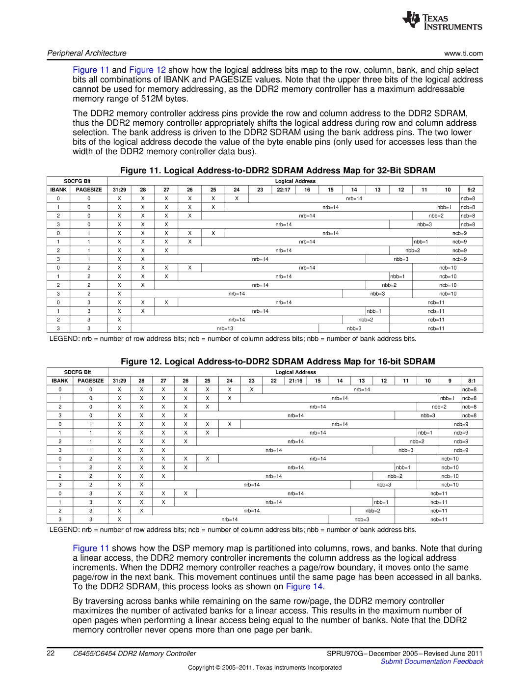
Figure 11 and Figure 12 show how the logical address bits map to the row, column, bank, and chip select bits all combinations of IBANK and PAGESIZE values. Note that the upper three bits of the logical address cannot be used for memory addressing, as the DDR2 memory controller has a maximum addressable memory range of 512M bytes.
The DDR2 memory controller address pins provide the row and column address to the DDR2 SDRAM, thus the DDR2 memory controller appropriately shifts the logical address during row and column address selection. The bank address is driven to the DDR2 SDRAM using the bank address pins. The two lower bits of the logical address decode the value of the byte enable pins (only used for accesses less than the width of the DDR2 memory controller data bus).
Figure 11. Logical Address-to-DDR2 SDRAM Address Map for 32-Bit SDRAM
SDCFG Bit |
|
|
|
|
|
|
|
| Logical Address |
|
|
|
|
|
|
|
|
|
|
| ||
|
|
|
|
|
|
|
|
|
|
|
|
|
|
|
|
|
|
|
|
|
| |
IBANK | PAGESIZE | 31:29 | 28 | 27 | 26 | 25 |
| 24 | 23 | 22:17 | 16 | 15 | 14 | 13 |
| 12 |
| 11 |
| 10 |
| 9:2 |
0 | 0 | X | X | X | X | X |
| X |
|
|
|
| nrb=14 |
|
|
|
|
|
|
|
| ncb=8 |
|
|
|
|
|
|
|
|
|
|
|
|
|
|
|
|
|
|
|
|
|
|
|
1 | 0 | X | X | X | X | X |
|
|
|
|
| nrb=14 |
|
|
|
|
|
|
| nbb=1 |
| ncb=8 |
|
|
|
|
|
|
|
|
|
|
|
|
|
|
|
|
|
|
|
|
|
|
|
2 | 0 | X | X | X | X |
|
|
|
|
| nrb=14 |
|
|
|
|
|
|
| nbb=2 |
| ncb=8 | |
3 | 0 | X | X | X |
|
|
|
|
| nrb=14 |
|
|
|
|
|
|
| nbb=3 |
| ncb=8 | ||
|
|
|
|
|
|
|
|
|
|
|
|
|
|
|
|
|
|
|
|
|
|
|
0 | 1 | X | X | X | X | X |
|
|
|
|
| nrb=14 |
|
|
|
|
|
|
|
| ncb=9 | |
|
|
|
|
|
|
|
|
|
|
|
|
|
|
|
|
|
|
|
|
|
| |
1 | 1 | X | X | X | X |
|
|
|
|
| nrb=14 |
|
|
|
|
|
| nbb=1 |
| ncb=9 | ||
2 | 1 | X | X | X |
|
|
|
|
| nrb=14 |
|
|
|
|
|
| nbb=2 |
|
| ncb=9 | ||
|
|
|
|
|
|
|
|
|
|
|
|
|
|
|
|
|
|
|
|
| ||
3 | 1 | X | X |
|
|
|
|
| nrb=14 |
|
|
|
|
|
| nbb=3 |
|
| ncb=9 | |||
|
|
|
|
|
|
|
|
|
|
|
|
|
|
|
|
|
|
|
|
|
| |
0 | 2 | X | X | X | X |
|
|
|
|
| nrb=14 |
|
|
|
|
|
|
|
| ncb=10 | ||
1 | 2 | X | X | X |
|
|
|
|
| nrb=14 |
|
|
|
|
| nbb=1 |
|
|
| ncb=10 | ||
|
|
|
|
|
|
|
|
|
|
|
|
|
|
|
|
|
|
|
|
|
| |
2 | 2 | X | X |
|
|
|
|
| nrb=14 |
|
|
|
|
| nbb=2 |
|
|
| ncb=10 | |||
|
|
|
|
|
|
|
|
|
|
|
|
|
|
|
|
|
|
|
| |||
3 | 2 | X |
|
|
|
|
| nrb=14 |
|
|
|
|
| nbb=3 |
|
|
| ncb=10 | ||||
0 | 3 | X | X | X |
|
|
|
|
| nrb=14 |
|
|
|
|
|
|
|
| ncb=11 |
|
| |
|
|
|
|
|
|
|
|
|
|
|
|
|
|
|
|
|
|
|
|
|
|
|
1 | 3 | X | X |
|
|
|
|
| nrb=14 |
|
|
|
| nbb=1 |
|
|
|
| ncb=11 |
|
| |
|
|
|
|
|
|
|
|
|
|
|
|
|
|
|
|
|
|
|
|
|
|
|
2 | 3 | X |
|
|
|
|
| nrb=14 |
|
|
|
| nbb=2 |
|
|
|
| ncb=11 |
|
| ||
3 | 3 | X |
|
|
|
| nrb=13 |
|
|
|
| nbb=3 |
|
|
|
|
| ncb=11 |
|
| ||
|
|
|
|
|
|
|
|
|
|
|
|
|
|
|
|
|
|
|
|
|
|
|
LEGEND: nrb = number of row address bits; ncb = number of column address bits; nbb = number of bank address bits.
Figure 12. Logical Address-to-DDR2 SDRAM Address Map for 16-bit SDRAM
SDCFG Bit |
|
|
|
|
|
|
| Logical Address |
|
|
|
|
|
|
| |||
|
|
|
|
|
|
|
|
|
|
|
|
|
|
|
|
|
|
|
IBANK | PAGESIZE | 31:29 | 28 | 27 | 26 | 25 | 24 | 23 | 22 | 21:16 | 15 | 14 | 13 | 12 | 11 | 10 | 9 | 8:1 |
|
|
|
|
|
|
|
|
|
|
|
|
|
|
|
|
|
|
|
0 | 0 | X | X | X | X | X | X | X |
|
|
|
| nrb=14 |
|
|
|
| ncb=8 |
|
|
|
|
|
|
|
|
|
|
|
|
|
|
|
|
|
|
|
1 | 0 | X | X | X | X | X | X |
|
|
|
| nrb=14 |
|
|
|
| nbb=1 | ncb=8 |
|
|
|
|
|
|
|
|
|
|
|
|
|
|
|
|
|
|
|
2 | 0 | X | X | X | X | X |
|
|
|
| nrb=14 |
|
|
|
| nbb=2 | ncb=8 | |
|
|
|
|
|
|
|
|
|
|
|
|
|
|
|
|
|
|
|
3 | 0 | X | X | X | X |
|
|
|
| nrb=14 |
|
|
|
|
| nbb=3 |
| ncb=8 |
|
|
|
|
|
|
|
|
|
|
|
|
|
|
|
|
|
|
|
0 | 1 | X | X | X | X | X | X |
|
|
|
| nrb=14 |
|
|
|
| ncb=9 | |
|
|
|
|
|
|
|
|
|
|
|
|
|
|
|
|
|
|
|
1 | 1 | X | X | X | X | X |
|
|
|
| nrb=14 |
|
|
|
| nbb=1 | ncb=9 | |
|
|
|
|
|
|
|
|
|
|
|
|
|
|
|
|
|
|
|
2 | 1 | X | X | X | X |
|
|
|
| nrb=14 |
|
|
|
| nbb=2 | ncb=9 | ||
|
|
|
|
|
|
|
|
|
|
|
|
|
|
|
|
|
|
|
3 | 1 | X | X | X |
|
|
|
| nrb=14 |
|
|
|
|
| nbb=3 |
| ncb=9 | |
|
|
|
|
|
|
|
|
|
|
|
|
|
|
|
|
|
|
|
0 | 2 | X | X | X | X | X |
|
|
|
| nrb=14 |
|
|
|
|
| ncb=10 |
|
|
|
|
|
|
|
|
|
|
|
|
|
|
|
|
|
|
|
|
1 | 2 | X | X | X | X |
|
|
|
| nrb=14 |
|
|
|
| nbb=1 |
| ncb=10 |
|
|
|
|
|
|
|
|
|
|
|
|
|
|
|
|
|
|
|
|
2 | 2 | X | X | X |
|
|
|
| nrb=14 |
|
|
|
| nbb=2 |
| ncb=10 |
| |
|
|
|
|
|
|
|
|
|
|
|
|
|
|
|
|
|
|
|
3 | 2 | X | X |
|
|
|
| nrb=14 |
|
|
|
|
| nbb=3 |
|
| ncb=10 |
|
|
|
|
|
|
|
|
|
|
|
|
|
|
|
|
|
|
|
|
0 | 3 | X | X | X | X |
|
|
|
| nrb=14 |
|
|
|
|
| ncb=11 |
| |
|
|
|
|
|
|
|
|
|
|
|
|
|
|
|
|
|
|
|
1 | 3 | X | X | X |
|
|
|
| nrb=14 |
|
|
|
| nbb=1 |
| ncb=11 |
| |
|
|
|
|
|
|
|
|
|
|
|
|
|
|
|
|
|
|
|
2 | 3 | X | X |
|
|
|
| nrb=14 |
|
|
|
| nbb=2 |
| ncb=11 |
| ||
|
|
|
|
|
|
|
|
|
|
|
|
|
|
|
|
|
|
|
3 | 3 | X |
|
|
|
| nrb=14 |
|
|
|
|
| nbb=3 |
|
| ncb=11 |
| |
|
|
|
|
|
|
|
|
|
|
|
|
|
|
|
|
|
|
|
LEGEND: nrb = number of row address bits; ncb = number of column address bits; nbb = number of bank address bits.
Figure 11 shows how the DSP memory map is partitioned into columns, rows, and banks. Note that during a linear access, the DDR2 memory controller increments the column address as the logical address increments. When the DDR2 memory controller reaches a page/row boundary, it moves onto the same page/row in the next bank. This movement continues until the same page has been accessed in all banks. To the DDR2 SDRAM, this process looks as shown on Figure 14.
By traversing across banks while remaining on the same row/page, the DDR2 memory controller maximizes the number of activated banks for a linear access. This results in the maximum number of open pages when performing a linear access being equal to the number of banks. Note that the DDR2 memory controller never opens more than one page per bank.
22 | C6455/C6454 DDR2 Memory Controller | SPRU970G – December 2005 – Revised June 2011 |
|
| Submit Documentation Feedback |
Copyright ©