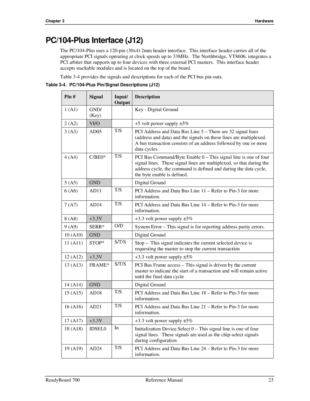
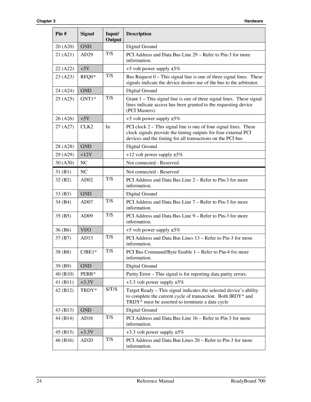
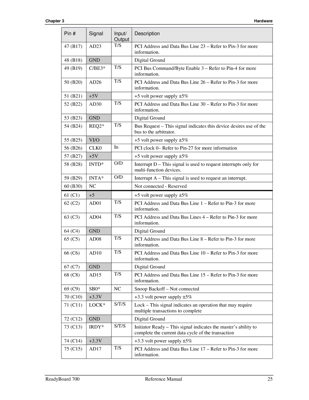
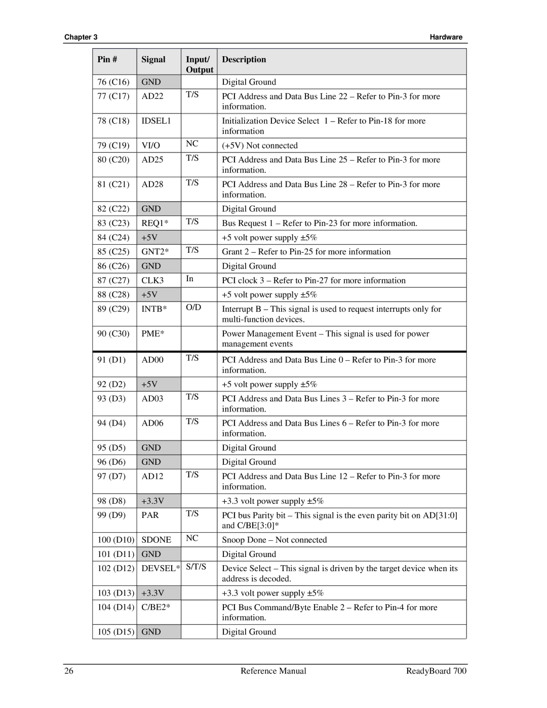
Ampro Corporation 700 manual CompactFlash Adapter J23

Page 41

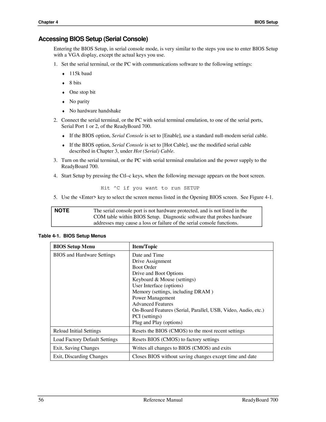
Chapter 3

Hardware

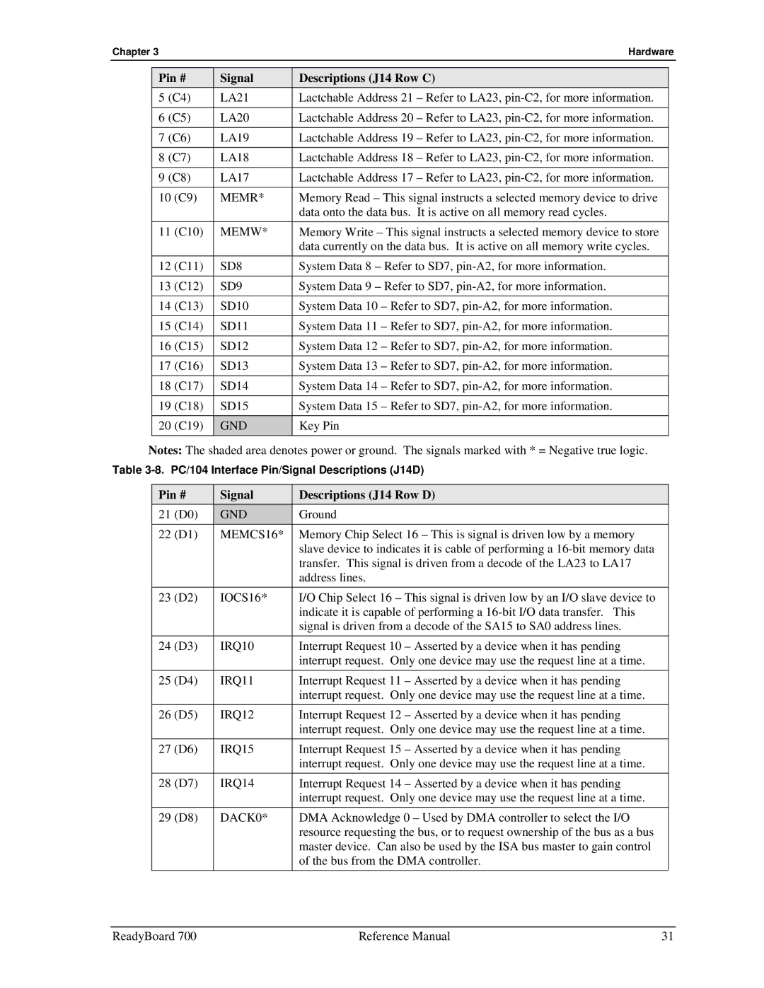
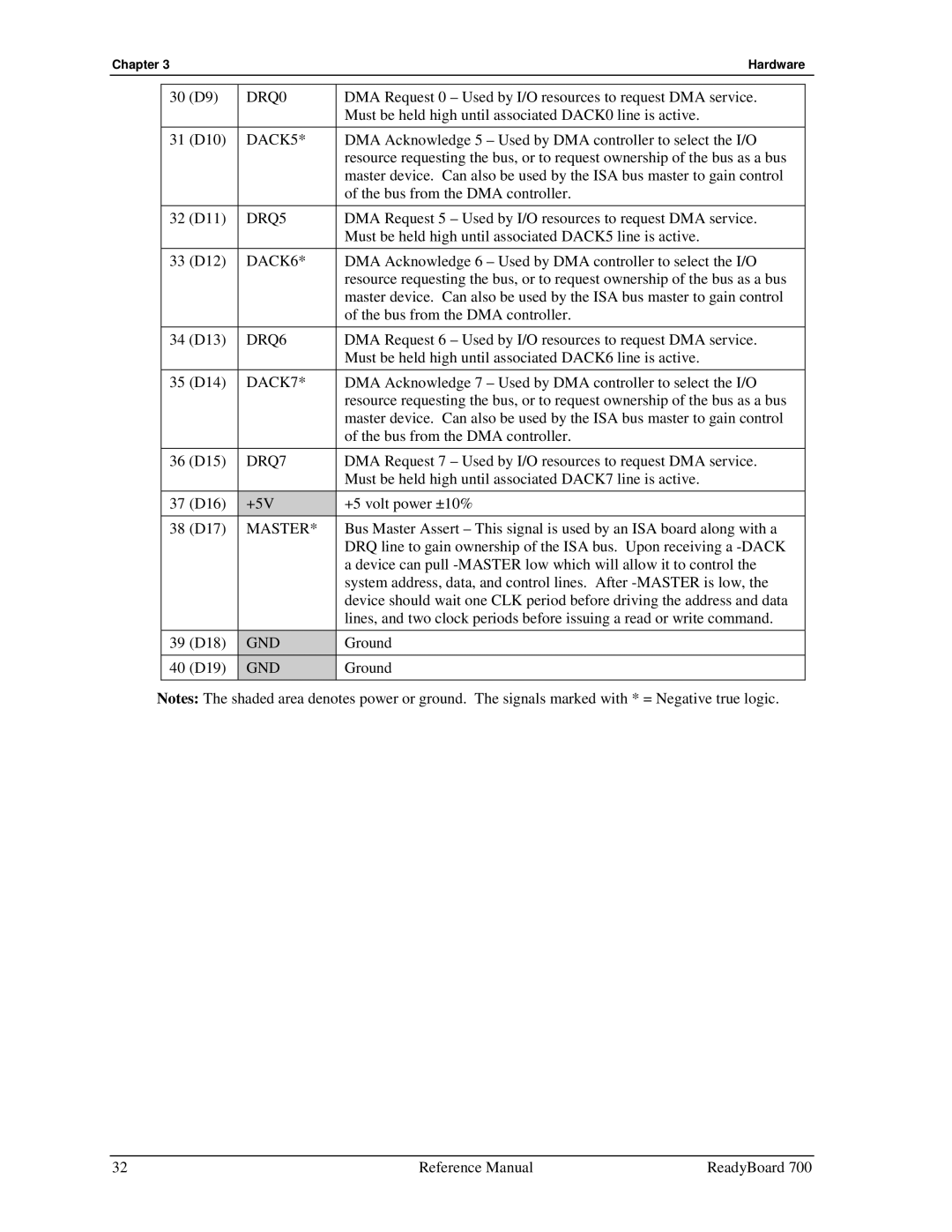
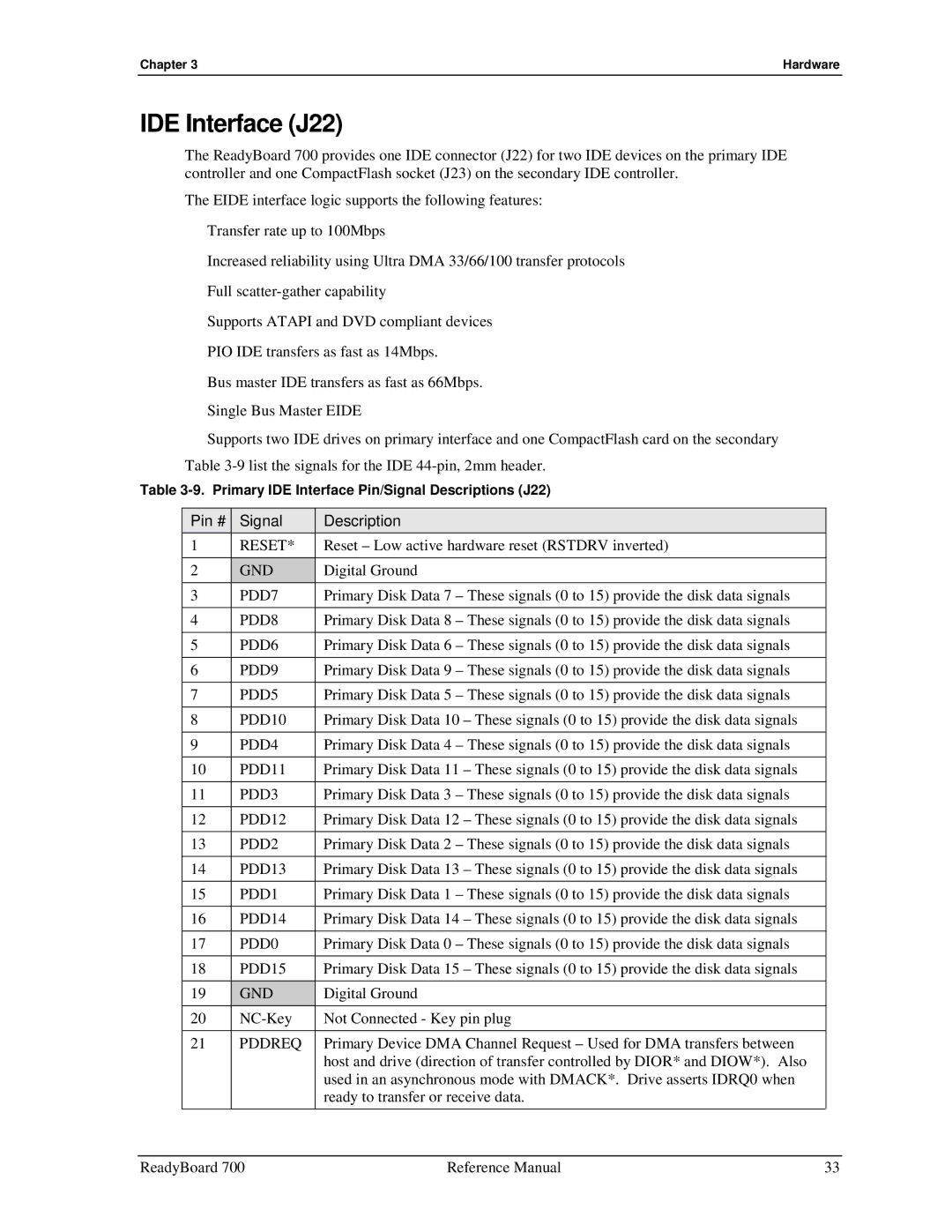
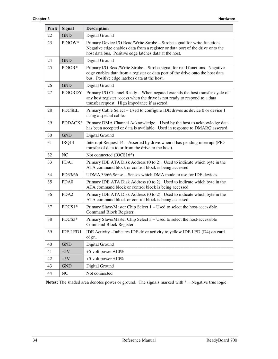
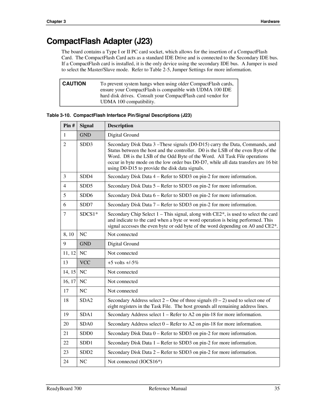
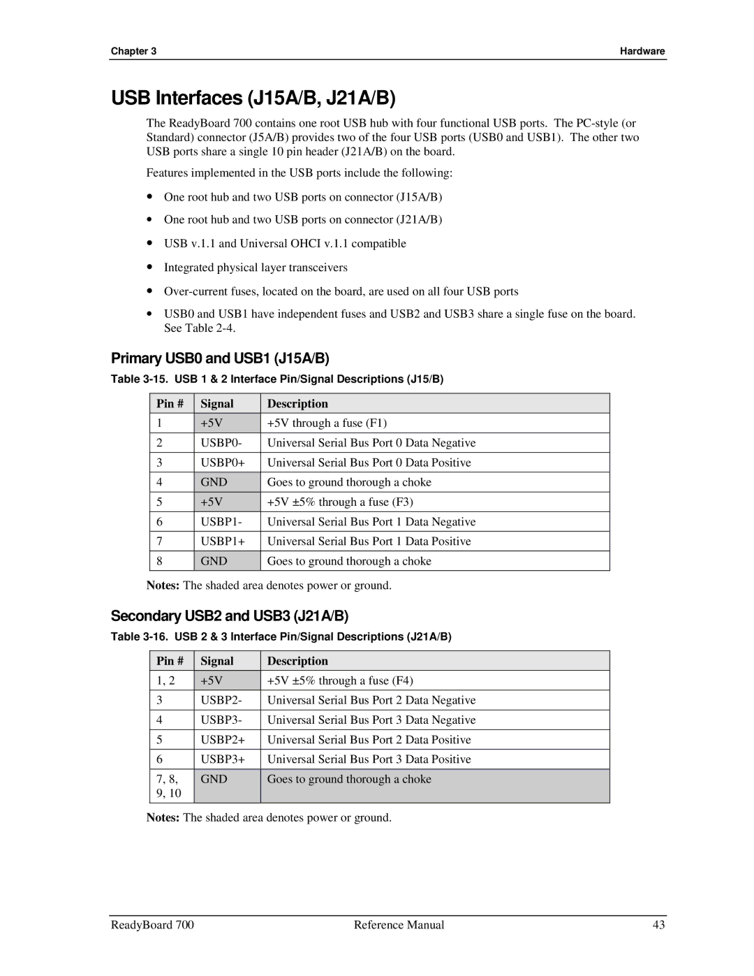
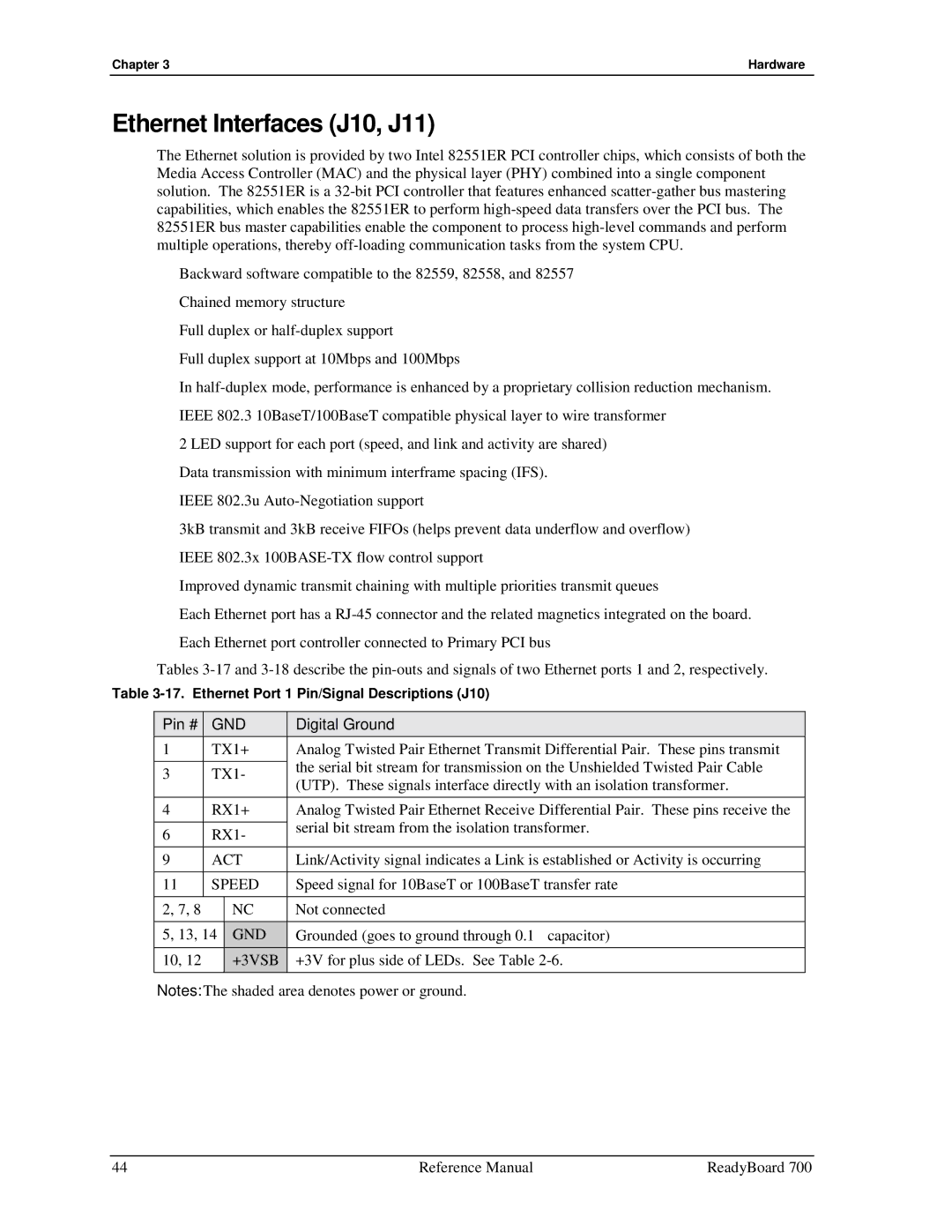
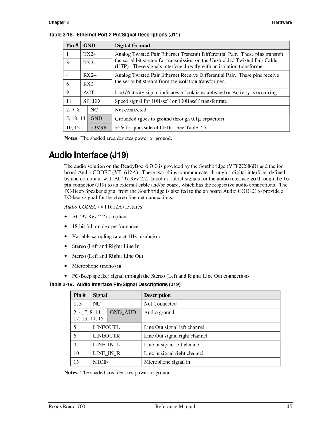
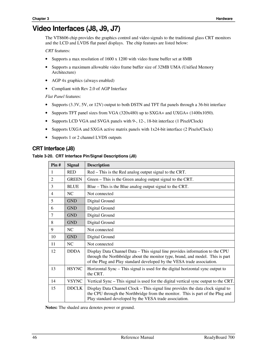
CompactFlash Adapter (J23)

The board contains a Type I or II PC card socket, which allows for the insertion of a CompactFlash Card. The CompactFlash Card acts as a standard IDE Drive and is connected to the Secondary IDE bus. If a CompactFlash card is installed, it is the only device using the secondary IDE bus. A Jumper is used to select the Master/Slave mode. Refer to Table 2-5, Jumper Settings for more information.

CAUTION To prevent system hangs when using older CompactFlash cards, ensure your CompactFlash is compatible with UDMA 100 IDE hard disk drives. Consult your CompactFlash card vendor for UDMA 100 compatibility.

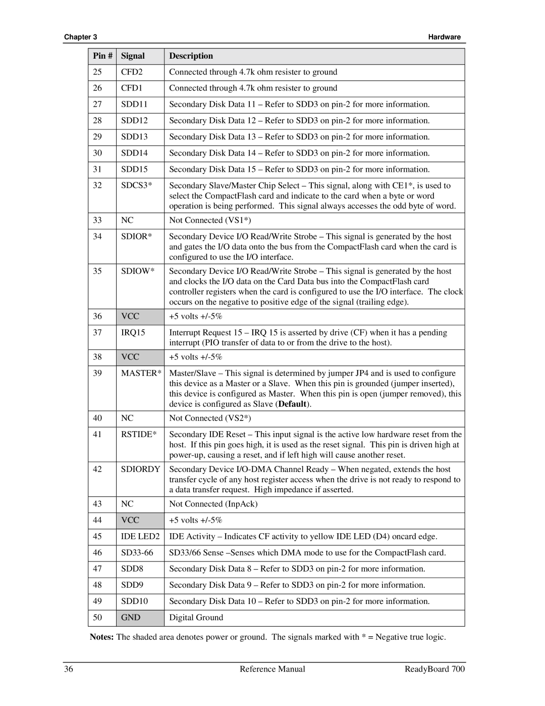
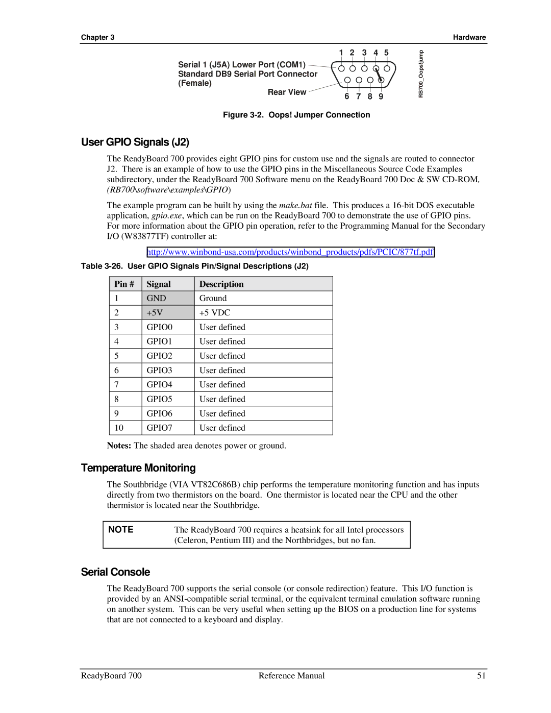
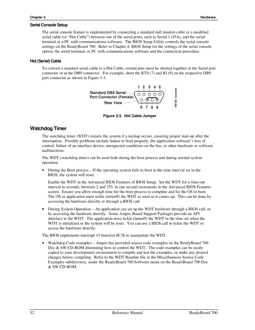
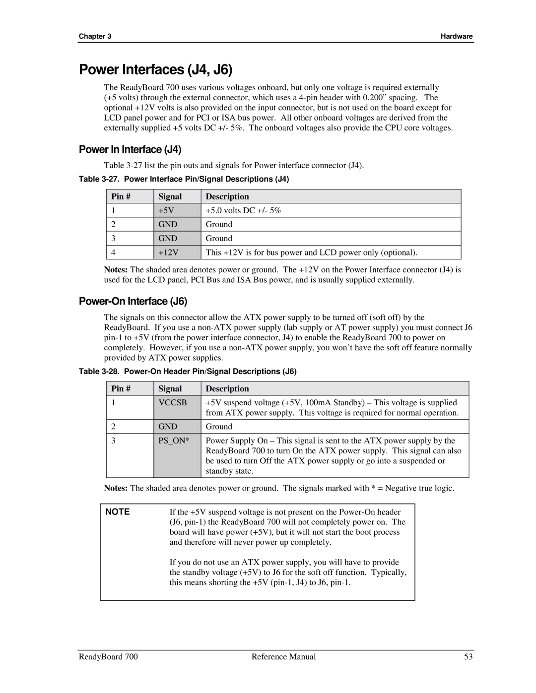
Table 3-10. CompactFlash Interface Pin/Signal Descriptions (J23)

Pin #

Signal

Description


1

GND

Digital Ground


2

SDD3

Secondary Disk Data 3 –These signals (D0-D15) carry the Data, Commands, and


Status between the host and the controller. D0 is the LSB of the even Byte of the


Word. D8 is the LSB of the Odd Byte of the Word. All Task File operations


occur in byte mode on the low order bus D0-D7, while all data transfers are 16 bit


using D0-D15 to provide the disk data signals.

3

SDD4

Secondary Disk Data 4 – Refer to SDD3 on pin-2 for more information.


4

SDD5

Secondary Disk Data 5 – Refer to SDD3 on pin-2 for more information.


5

SDD6

Secondary Disk Data 6 – Refer to SDD3 on pin-2 for more information.


6

SDD7

Secondary Disk Data 7 – Refer to SDD3 on pin-2 for more information.


7

SDCS1*

Secondary Chip Select 1 – This signal, along with CE2*, is used to select the card


and indicate to the card when a byte or word operation is being performed. This


signal accesses the even byte or odd byte of the word depending on A0 and CE2*.

8, 10

NC

Not connected


9

GND

Digital Ground


11, 12

NC

Not connected


13

VCC

+5 volts +/-5%


14, 15

NC

Not connected


16, 17

NC

Not connected


17

NC

Not connected


18

SDA2

Secondary Address select 2 – One of three signals (0 – 2) used to select one of


eight registers in the Task File. The host grounds all remaining address lines.

19

SDA1

Secondary Address select 1 – Refer to A2 on pin-18 for more information.


20

SDA0

Secondary Address select 0 – Refer to A2 on pin-18 for more information.


21

SDD0

Secondary Disk Data 0 – Refer to SDD3 on pin-2 for more information.


22

SDD1

Secondary Disk Data 1 – Refer to SDD3 on pin-2 for more information.


23

SDD2

Secondary Disk Data 2 – Refer to SDD3 on pin-2 for more information.


24

NC

Not connected (IOCS16*)


ReadyBoard 700

Reference Manual

35

Image 41
Contents ReadyBoard Single Board Computer Reference Manual Revision History Audience AssumptionsContents Appendix a List of Tables Reference Manual ReadyBoard Reference Material SpecificationsPurpose of this Manual ReadyBoard 700 Support Products Related Ampro ProductsOther ReadyBoard Products Other Ampro ProductsChapter Reference Manual ReadyBoard Epic Architecture Product OverviewProduct Description Board FeaturesChapter Chapter ATA Block DiagramChip Type Mfg Model Description Function Major Integrated Circuits ICsCPU VIASwitch Definition Connector DefinitionsJack # Signal/Device Description Component DescriptionLvds J7 All illustrationsIllustrations Additional ComponentsJumper # Installed Removed Power/IDE LED DefinitionsIndicator Definition Jumper DefinitionsJumper, Switch, and LED Locations Top view Physical Specifications SpecificationsPower Specifications Environmental SpecificationsThermal/Cooling Requirements Mechanical SpecificationsReadyBoard 700 Side view Overview Chapter HardwareMemory CPU U4Sdram Memory DIMM1 Flash MemoryMemory Map Interrupt Channel AssignmentsBase Address Function Address MapAddress hex Subsystem CF8-CFFPC/104-Plus Interface J12 Pin # Signal Input Description OutputGNT1 REQ0CLK2 PerrCLK0 REQ2Intd IntaREQ1 IDSEL1GNT2 CLK3IDSEL3 IDSEL2GNT0 CLK1PC/104 Interface J13 A/B, J14 C/D Pin # Signal Description J13 Row aPin # Signal Descriptions J13 Row B Pin # Signal Descriptions J14 Row C Pin # Signal Descriptions J14 Row D DACK5 DRQ0DRQ5 DACK6IDE Interface J22 Pin # Signal DescriptionPdior PdiowPdiordy PdcselCompactFlash Adapter J23 CFD1 CFD2SDD11 SDD12Floppy/Parallel Interface J20 Step SlctinAutofdx DrvenoRS485 Serial Port Implementation Serial Interfaces J5A/B, J3A/BSerial a Interface J5A/B Serial B Interface J3A/B DTR4 CTS4Secondary USB2 and USB3 J21A/B USB Interfaces J15A/B, J21A/BPrimary USB0 and USB1 J15A/B Digital Ground Ethernet Interfaces J10, J11Pin # Audio Interface J19 CRT Interface J8 Video Interfaces J8, J9, J7LCD Interface J9 Lvds Interface J7 Pin # Signal Description Line ChannelMiscellaneous Reset Switch SW1Utility Interface J18 Keyboard/Mouse Interface J16Infrared IrDA Port J17 Oops! Jumper Bios RecoveryReal Time Clock RTC IrtxSerial Console User Gpio Signals J2Temperature Monitoring Serial Console Setup Watchdog TimerPower In Interface J4 Power Interfaces J4, J6Power-On Interface J6 VccsbReference Manual ReadyBoard Introduction Accessing Bios Setup VGA DisplayBios Setup Menu Item/Topic Accessing Bios Setup Serial ConsoleBios Setup Opening Screen Bios MenusDrive Assignments Bios Configuration ScreenDate & Time Boot Order # of Floppy Drives Bios SettingsDrive and Boot Options Memory Keyboard and Mouse ConfigurationUser Interface Advanced features Power ManagementChapter Bios Setup On-Board LPT Port On-Board Serial PortsOn-Board Video On-Board ControllersPanel Type 640 x 480 x 18 TFT LCD ResolutionType 640 x 480 x 18 bitChapter Bios Setup Chapter Bios Setup Chapter Bios Setup Converting the Splash Screen File Splash Screen CustomizationSplash Screen Image Requirements \splashconvert convert.idf Reference Manual ReadyBoard Method Contact Information Appendix a Technical SupportAppendix a Appendix B LAN Boot Option Accessing PXE Boot Agent Bios Setup PXE Boot Agent Bios SetupTCP/IP Configuration PXE Boot Agent Setup ScreenPXE Configuration RPL Configuration NetWare ConfigurationLED CD-ROMPost RTCWatchdog timer WDT Table notes Reference Manual ReadyBoard