Assembly Level Repair
Agilent Part No January
Page
Introduction
Repairing the HP/Agilent
Book Organization
Introduction
Contents
Adjustments and Calibration
Troubleshooting the Power Supply
Assembly and Disassembly Procedures
Service Screen
Self-Test Error Messages
Replacing a Part
Module I/O Specifications
Instrument Block Diagrams
Block Diagram Theory of Operation
GSM Theory
Measurement Theory
Index
Contents-6
Localizing the Problem
Localizing the Problem
Localizing the Problem Flow Chart Power-Up
Localizing the Problem Flow Chart
Power-Up Checks
Power-Up Checks Agilent
Error Message Numbers
If Power-Up Checks Failed
Error Message Numbers Failure Suspect Assembly
Power-Up Self Test Diagnostics
Self Test LED Location
LED Conventions
LED Sequences
No Failures
Failure Detected
Sequence of LED Patterns
Where to Go Next
If Power-Up Happened Correctly
Front Panel Connections
Where to Go Next
RF Analyzer Settings
Checking the RF Analyzer Using the RF Generator
Front Panel Connections for the RF Analyzer
RF Generator/Analyzer Settings
CW Readings
Checking the AF Analyzer using the AF Generator
Related to the RF Analyzer
Front Panel Connections for the Audio Check
Checking the AF Analzyer Using the AF Generator
Audio Measurements
If Power-Up Happened Correctly
Running Diagnostics
Running Diagnostics
Running Memory Card or ROM Based Diagnostics
Afdiags RFDIAGS1 MSDIAGS1 Calrev Loopback
Reading Memory Card Diagnostic Test Results
Probability Indicator
Selecting Memory Card Diagnostic Test Execution Conditions
Before Running a Test While Running a Test
Loading the RAM Test
Loading and Running the Ram Test
Selecting from a List
This Page Intentionally Left Blank
Verifying Performance
Installing and Operating the Software
Verification
Performace Test Software
Understanding the Tests
Back Conversion
To Load the Program in the Agilent 8922M/S
Forward Conversion
To Configure the Gpib Addresses
To Run the Program
Using the HP/Agilent 83210A Service Kit
Using the HP/Agilent 83210A Service Kit
Configuring the RF Extender
Coax Jumpers for RF Extender Board
RF Extender Board
Extender Board Part Numbers
Extending Modules
REF # Description Extender
Making Measurements
Audio / Digital Assemblies
Making Measurements
This Page Intentionally Left Blank
Troubleshooting the Controller/Display
Troubleshooting the Controller/Display
Parallel Bus
Serial Bus
Display
Line Name Pin Number Description
Keyboard
Parenthesis Column Pin
Where to Go Next
This Page Intentionally Left Blank
Troubleshooting the Power Supply
Troubleshooting the Power Supply
Power Cord Verification
8120-2956 90/Straight
Line Voltage Selection / Line Fuse Replacement
Transformer / Power Switch
A28 Power Supply
Where To Go Next
Adjustments and Calibration
Adjustments and Calibration
Timebase Adjustments
Standard Timebase Adjustment Procedure Reference Calibration
Option 001 High Stability Timebase Adjustment Procedure
High Stability Timebase Adjustment
Periodic Calibrations
To Run the Periodic Self-Calibration Program
Procedure
Sum Loop Adjustment Procedure
First Adjustment
Final Adjustment
Second Adjustment
Final Check
This Page Intentionally Left Blank
Assembly and Disassembly Procedures
Recommended Torque
Further Information
Top and Bottom Cover Removal
Tools Required
Inside Protective Covers
AF, Digital and RF Assemblies Removal
Release Levers Pull Ring
Disconnecting Cables
A1 Front Panel Removal
Removing Modules
Detaching Front Panel
A1 Mounting Screws
A10 Power Supply Regulator Removal
A11 Receiver Mixer Removal
TOP View Mixer Side View
A12 Pulse Attenuator Removal
TOP View Pulse Switch Side View
A21 Gpib Interface Removal
TOP View
A22 Display Removal
CRT
A23 Input Section Removal
A24 Attenuator Removal
A28 Power Supply Removal
A28 Power Supply Removal
Fan Removal
Fan Removal
Transformer Removal
Replacing a Part
Assembly Replacements
Adjustments after Replacing Assemblies
Adjustments After Replacement
Assembly Calibration or Adjustment Replaced Required
Replaceable Parts
Replaceable Parts
Agilent Part Qty. Description Mfr. Code Mfr.Part Number
A1 Mounting Screws
Agilent Part Qty Description Mfr Mfr.Part Number Code
Replaceable Parts
MOD-PCB REF Section
Replaceable Parts
Agilent Part Qty Description Mfr. Code Mfr.Part Number
Replaceable Parts
BRACKET-TIMEBASE
Replaceable Parts
Cable Ribbon CRT-MBOARD
Ribbon 16 CND
Replaceable Parts
Replaceable Parts
TOP Flange
Replaceable Parts
AY-FRAME, Chassis
Replaceable Parts
Washer .375 OD
Replaceable Parts
Mfr. Code Mfr.Part Number
79-82, 108-111
Serial Prefix 3235A and Below 8922E All Prefixes
Replaceable Parts
Miscellaneous Replaceable Parts
Firmware Upgrades
Agilent 8922M
HP/Agilent 8922A, B, E, G, F, H, S
HP Part Number Description
This Page Intentionally Left Blank
Service Screen
Frequency
Voltage
Voltmeter Connection
Counter Connection
Gate Time
Latch
Value
10-4
Self-Test Error Messages
Self-Test Error Messages
Module I/O Specifications
Module I/O Specifications
Power Supplies
A2 Audio Analyzer
Inputs
Audio Input MUX
Audio OUT Meas MUX
Outputs
Speaker
A3 Audio Analyzer
Audio Input MUX Demodaud J16
Extscope J111
Audinhi J11
Filaud J115
Selected Inputs AUDINHI,AUDINLO
AUD1VM J116
Selected input =Range/Over-voltage detector
Selected input = DC Audio Path
Dcaudio J1
Extmod J11
A4 Modulation Distribution
AFG1 J111, AFG2 J113, Afggnd J112
Ammod J120
Audioouthi J17
Modmon J118
A5 Premodulation Filter and NSM
Pmfclk J15
MHz Ref B J233
Pmfdata J11
Nsmifclk J21
Typical Oscilloscope Display
Serial I/O
Hop Control
A6 Signaling Source/Analyzer
Procaud J111
AFG1 J13, AFG2 J15
A9 Global Test and Demod
10.7MIF J17
Expected Output
20MREFA J111
Expected Display
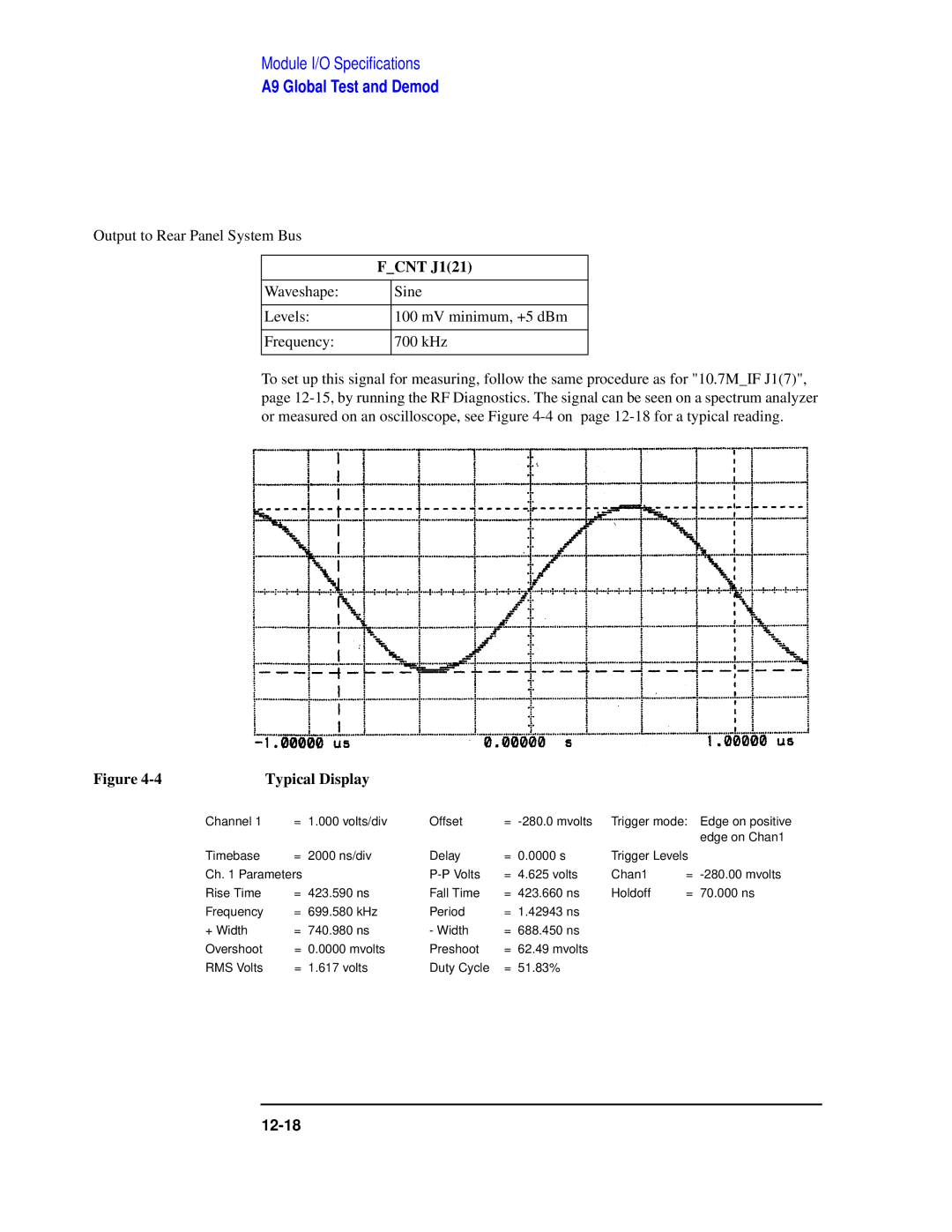
Fcnt J121
Typical Display
1stMIXIN J2
A11 Receiver Mixer
Extrefin J1
12-20
Rcvrin J3
A13 Output
Inputs2
Coax jumper connection SGS50010000M J117
Coax jumper connection OUT1GREF J13
Ammod J27
Coax jumper connection Mainrfout J313
Output Level
Spectral Purity Only contributions of the outputmodule
A14 Pulse Driver
1MREFC P33
13MREFOUTA P317
13MREFOUTB
Attenselect
P1 11, 13, 15, 17
Exrefin J19
A15 Reference
13MOUTLOCK J27
Hop Control
J25,8,9
EX10MREFOUT J113
1MREFA P34
1MREFC J32
MEAS20MREF J313
SA20MREF J35
10MREFC J39
20MREFA J320
10MREFB J317
OUT1GREF J13
1GDIAG J21
500MREF J117
500MDIAG J26
A16 Receiver
Hop Control P2,5,8
500MREF P33
Rcvrin J13
Unmutedfm J114
Pulsedemod J17
Demodaud J26
Fmdemod J113
10.7MIF J39
SA114.3M J313
AUX7VM J27
SA114.3M P317
A18 Spectrum Analyzer
SA20MREF J13
Swpstrt J16
Sascpt J17
A19 Measurement
Voltmeter Multiplexer
Intemp J34 Involt J35
12-40
12-41
Signscptrig J110 Riscptrig J17 Exttrig J14
Trigger Input Scope Trigger Internal
Internal Trigger Internal
AUX RF Input J3
A23 Input HP/Agilent 8922A.B,E,F,G,H Only
SG in J4
AUX RF OUT J2
RF IN/OUT Output J1
DET LO J614
1stMIXIN J5
Involt J615
Duplexdet
A23 Input Agilent 8922M/S Only
12-48
12-49
Dacupout J33
A25 Sum Loop
Sumlpptune J27
Sumlock J21
STEPLPOUT/A J317
AUX3VM J26
SGS5001000M J13
A17, A26 Step Loop
1MREFA/B P33
Hop Control J25,8,9
Steplpout J13
AUX1/2VM J26
Nsmifclk J12
A27 DAC/Upconverter
Nsmifdata J15-16
AUX4-VM J26
MHz Ref C J119
Dacupout J315
Input
Hop Control Input Bus Hopaddr J215-15
A33 Hop Controller
Txhop J214
Seqhopreset J211
Resetselect J2119
Rxhop J213
Seqhop J212
Pulsemodin J2168
Host Processor Interface
Seqtrigout J2121
EA60SW0/2 J2171,72,73
Premod Filter & NSM
J2125,23,26
Instrument Block Diagrams
Block Diagram
Reading the Pin Numbers
13-3
13-4
Block Diagram Theory of Operation
Block Diagram Theory of Operation
Technical Discussion
Block Diagram
A23 Input A24 High Power Attenuator
A17 StepLoop B
A11 Receiver Mixer
A16 Receiver
A9 Global Test and Demod
A18 Spectrum Aanalyzer
A2 Audio Analyzer 2 A3 Audio Analyzer
14-8
A15 Reference
A5 Premod Filter and NSM
14-10
A27 DAC/Upconverter
A26 Step Loop a
A25 Sum Loop
A13 Output
A23 Input A24 High Power Attenutor
A12 Pulse Attenuator
A4 Modulation Distribution A6 Signaling Source/Analyzer
Block Diagram HP/Agilent 8922B Only
A35 B Reference
A37 Sequence Controller
A32 GSM Controller
A35 Protocol Interface HP/Agilent 8922F/HM/S Option 003 Only
A19 Measurement
A33 Hop Controller
Diagnostics Theory
Diagnostics Theory
Audio Frequency Generators 1
Preliminary Audio Paths
Modulation Distribution Internal Paths
Modulation Distribution External Paths
Audio Analyzer 1 External Paths
Audio Analyzer 1 Internal Paths
Audio Analyzer
NSM and Pre-Modulation Filter
Reference
DAC and Up-Converter
Sum Loop
RF Generator Step Loop
Output Section
Pulse Attenuator and Drive
Input Section
RF Analyzer Step Loop
Spectrum Analyzer
Receiver
Temperature Test
Down Converters With Spectrum Analyzer Test
If Counter Test
AGC Open Loop At AM Output Test
RF Input/Output
External Reference
Instrument Self Test
GSM and DCS Diagnostic Tests
Interpreting Results
15-14
Measurement Theory
BIT Error
A31 Codec
OUT RF SP
DSP ANL
Pulse
Scope
CW MEAS/AF Analyzer
Spec ANL
16-5
16-6
GSM Theory
GSM Theory
GSM System
GSM, DCS1800 and PCS1900 Systems
Symbols
Numerics
Index-2
Index-3
Index-4
Index-5
Index-6