CY7C68033/CY7C68034
Pin Assignments
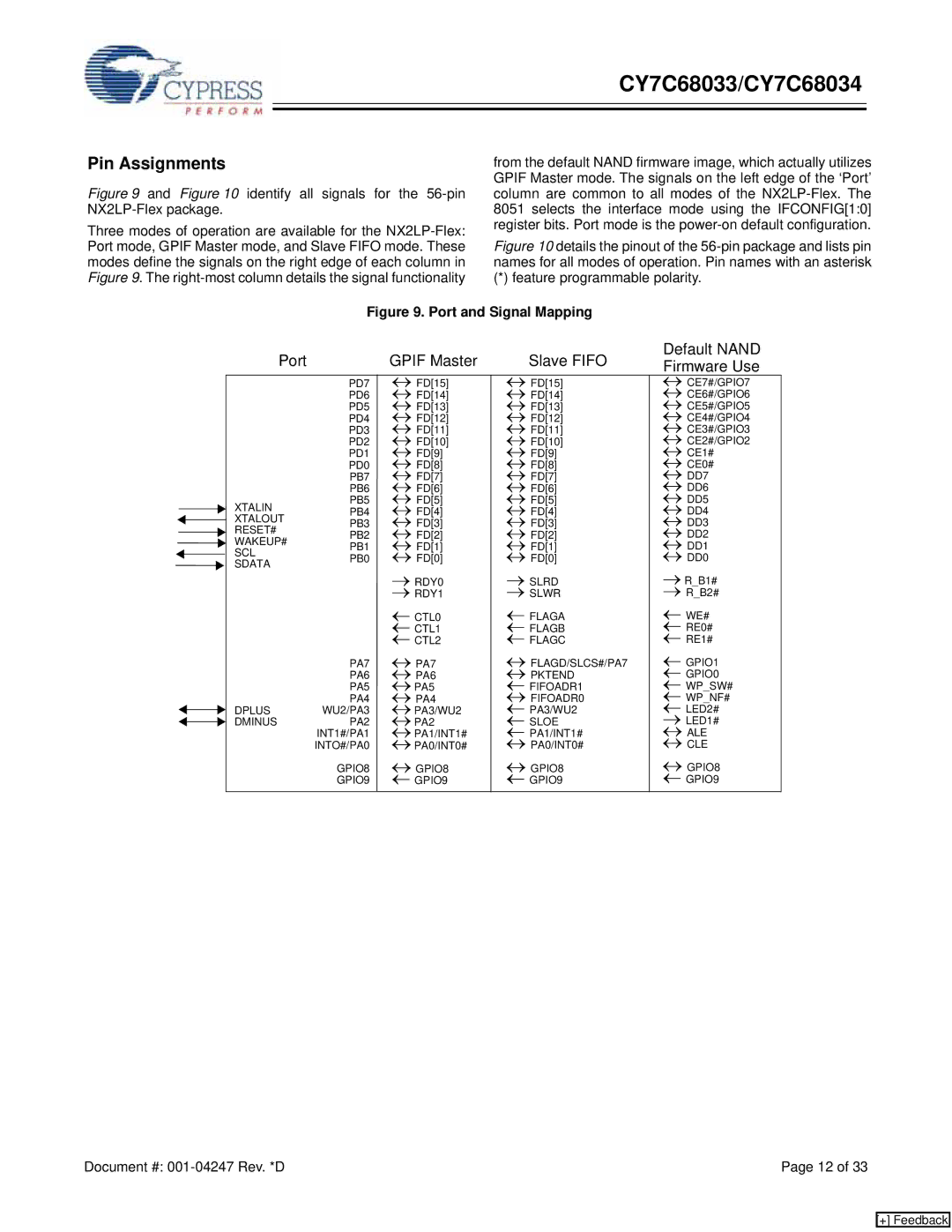
Figure 9 and Figure 10 identify all signals for the 56-pin NX2LP-Flex package.
Three modes of operation are available for the
from the default NAND firmware image, which actually utilizes GPIF Master mode. The signals on the left edge of the ‘Port’ column are common to all modes of the
Figure 10 details the pinout of the 56-pin package and lists pin names for all modes of operation. Pin names with an asterisk
(*) feature programmable polarity.
Figure 9. Port and Signal Mapping
|
|
|
| Port |
| GPIF Master |
| Slave FIFO |
| Default NAND | |
|
|
|
|
|
|
| Firmware Use | ||||
|
|
|
|
| PD7 | ↔ FD[15] |
| ↔ FD[15] |
| ↔ CE7#/GPIO7 |
|
|
|
|
|
|
|
|
| ||||
|
|
|
|
| PD6 | ↔ FD[14] |
| ↔ FD[14] |
| ↔ CE6#/GPIO6 |
|
|
|
|
|
| PD5 | ↔ FD[13] |
| ↔ FD[13] |
| ↔ CE5#/GPIO5 |
|
|
|
|
|
| PD4 | ↔ FD[12] |
| ↔ FD[12] |
| ↔ CE4#/GPIO4 |
|
|
|
|
|
| PD3 | ↔ FD[11] |
| ↔ FD[11] |
| ↔ CE3#/GPIO3 |
|
|
|
|
|
| PD2 | ↔ FD[10] |
| ↔ FD[10] |
| ↔ CE2#/GPIO2 |
|
|
|
|
|
| PD1 | ↔ FD[9] |
| ↔ FD[9] |
| ↔ CE1# |
|
|
|
|
|
| PD0 | ↔ FD[8] |
| ↔ FD[8] |
| ↔ CE0# |
|
|
|
|
|
| PB7 | ↔ FD[7] |
| ↔ FD[7] |
| ↔ DD7 |
|
|
|
|
|
| PB6 | ↔ FD[6] |
| ↔ FD[6] |
| ↔ DD6 |
|
|
|
|
|
| PB5 | ↔ FD[5] |
| ↔ FD[5] |
| ↔ DD5 |
|
|
|
|
| XTALIN | PB4 | ↔ FD[4] |
| ↔ FD[4] |
| ↔ DD4 |
|
|
|
|
|
|
|
| |||||
|
|
|
| XTALOUT | PB3 | ↔ FD[3] |
| ↔ FD[3] |
| ↔ DD3 |
|
|
|
|
|
|
| ||||||
|
|
|
| RESET# | PB2 | ↔ FD[2] |
| ↔ FD[2] |
| ↔ DD2 |
|
|
|
|
|
|
| ||||||
|
|
|
| WAKEUP# | PB1 | ↔ FD[1] |
| ↔ FD[1] |
| ↔ DD1 |
|
|
|
|
| SCL | PB0 | ↔ FD[0] |
| ↔ FD[0] |
| ↔ DD0 |
|
|
|
|
|
|
|
| |||||
|
|
|
| SDATA |
| → RDY0 |
| → SLRD |
| → R_B1# |
|
|
|
|
|
|
|
|
|
| |||
|
|
|
|
|
| → RDY1 |
| → SLWR |
| → R_B2# |
|
|
|
|
|
|
| ← CTL0 |
| ← FLAGA |
| ← WE# |
|
|
|
|
|
|
| ← CTL1 |
| ← FLAGB |
| ← RE0# |
|
|
|
|
|
|
| ← CTL2 |
| ← FLAGC |
| ← RE1# |
|
|
|
|
|
| PA7 | ↔ PA7 |
| ↔ FLAGD/SLCS#/PA7 |
| ← GPIO1 |
|
|
|
|
|
| PA6 | ↔ PA6 |
| ↔ PKTEND |
| ← GPIO0 |
|
|
|
|
|
| PA5 | ↔ PA5 |
| ← FIFOADR1 |
| ← WP_SW# |
|
|
|
|
|
| PA4 | ↔ PA4 |
| ↔ FIFOADR0 |
| ← WP_NF# |
|
|
|
|
| DPLUS | WU2/PA3 | ↔ PA3/WU2 |
| ← PA3/WU2 |
| ← LED2# |
|
|
|
|
|
|
| ||||||
|
|
|
| DMINUS | PA2 | ↔ PA2 |
| ← SLOE |
| → LED1# |
|
|
|
|
|
|
| ||||||
|
|
|
|
| INT1#/PA1 | ↔ PA1/INT1# |
| ← PA1/INT1# |
| ↔ ALE |
|
|
|
|
|
| INTO#/PA0 | ↔ PA0/INT0# |
| ↔ PA0/INT0# |
| ↔ CLE |
|
|
|
|
|
| GPIO8 | ↔ GPIO8 |
| ↔ GPIO8 |
| ↔ GPIO8 |
|
|
|
|
|
| GPIO9 | ← GPIO9 |
| ← GPIO9 |
| ← GPIO9 |
|
|
|
|
|
|
|
|
|
|
|
|
|
Document #: | Page 12 of 33 |
[+] Feedback