CY7C68033/CY7C68034
PCB Layout Recommendations[16]
The following recommendations should be followed to ensure reliable
•At least a
•Specify impedance targets (ask your board vendor what they can achieve) to meet USB specifications.
•To control impedance, maintain trace widths and trace spacing.
•Minimize any stubs to avoid reflected signals.
•Connections between the USB connector shell and signal ground must be done near the USB connector.
•Bypass/flyback caps on VBUS, near connector, are recom- mended.
•DPLUS and DMINUS trace lengths should be kept to within 2 mm of each other in length, with preferred length of
•Maintain a solid ground plane under the DPLUS and DMINUS traces. Do not allow the plane to be split under these traces.
•No vias should be placed on the DPLUS or DMINUS trace routing unless absolutely necessary.
•Isolate the DPLUS and DMINUS traces from all other signal traces as much as possible.
Quad Flat Package No Leads (QFN) Package Design Notes
Electrical contact of the part to the Printed Circuit Board (PCB) is made by soldering the leads on the bottom surface of the package to the PCB. Hence, special attention is required to the
heat transfer area below the package to provide a good thermal bond to the circuit board. A Copper (Cu) fill is to be designed into the PCB as a thermal pad under the package. Heat is transferred from the
For further information on this package design please refer to the application note Surface Mount Assembly of AMKOR’s MicroLeadFrame (MLF) Technology. This application note can be downloaded from AMKOR’s website from the following URL:
http://www.amkor.com/products/notes_papers/ MLF_AppNote_0902.pdf.
The application note provides detailed information on board mounting guidelines, soldering flow, rework process, etc.
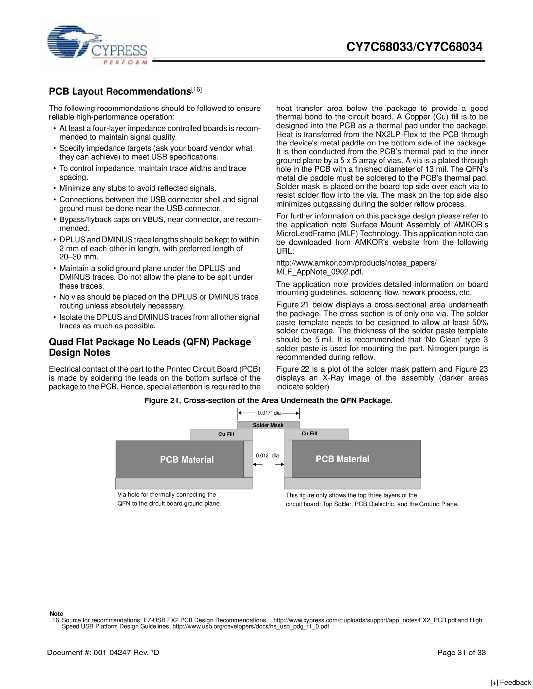
Figure 21 below displays a cross-sectional area underneath the package. The cross section is of only one via. The solder paste template needs to be designed to allow at least 50% solder coverage. The thickness of the solder paste template should be 5 mil. It is recommended that ‘No Clean’ type 3 solder paste is used for mounting the part. Nitrogen purge is recommended during reflow.
Figure 22 is a plot of the solder mask pattern and Figure 23 displays an X-Ray image of the assembly (darker areas indicate solder)
Figure 21. Cross-section of the Area Underneath the QFN Package.
![]()
![]() 0.017” dia
0.017” dia![]()
![]()
![]()
Solder Mask
Cu Fill
Cu Fill
PCB Material
Via hole for thermally connecting the QFN to the circuit board ground plane.
0.013” dia
PCB Material
This figure only shows the top three layers of the
circuit board: Top Solder, PCB Dielectric, and the Ground Plane.
Note
16.Source for recommendations:
Document #: | Page 31 of 33 |
[+] Feedback