CY7C68033/CY7C68034
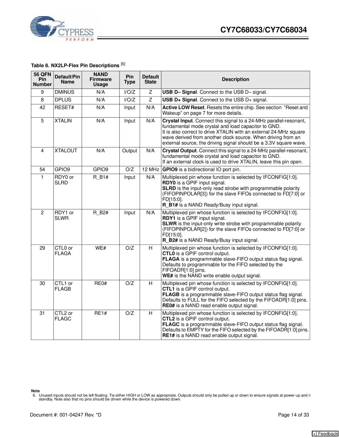
Table 8. NX2LP-Flex Pin Descriptions [6]
56 QFN | Default Pin | NAND | Pin | Default | Description |
Pin | Name | Firmware | Type | State | |
Number | Usage |
| |||
|
|
|
| ||
9 | DMINUS | N/A | I/O/Z | Z | USB D– Signal. Connect to the USB D– signal. |
8 | DPLUS | N/A | I/O/Z | Z | USB D+ Signal. Connect to the USB D+ signal. |
|
|
|
|
|
|
42 | RESET# | N/A | Input | N/A | Active LOW Reset. Resets the entire chip. See section ”Reset and |
|
|
|
|
| Wakeup” on page 7 for more details. |
5 | XTALIN | N/A | Input | N/A | Crystal Input. Connect this signal to a |
|
|
|
|
| fundamental mode crystal and load capacitor to GND. |
|
|
|
|
| It is also correct to drive XTALIN with an external |
|
|
|
|
| wave derived from another clock source. When driving from an |
|
|
|
|
| external source, the driving signal should be a 3.3V square wave. |
4 | XTALOUT | N/A | Output | N/A | Crystal Output. Connect this signal to a |
|
|
|
|
| fundamental mode crystal and load capacitor to GND. |
|
|
|
|
| If an external clock is used to drive XTALIN, leave this pin open. |
54 | GPIO9 | GPIO9 | O/Z | 12 MHz | GPIO9 is a bidirectional IO port pin. |
|
|
|
|
|
|
1 | RDY0 or | R_B1# | Input | N/A | Multiplexed pin whose function is selected by IFCONFIG[1:0]. |
| SLRD |
|
|
| RDY0 is a GPIF input signal. |
|
|
|
|
| SLRD is the |
|
|
|
|
| (FIFOPINPOLAR[3]) for the slave FIFOs connected to FD[7:0] or |
|
|
|
|
| FD[15:0]. |
|
|
|
|
| R_B1# is a NAND Ready/Busy input signal. |
2 | RDY1 or | R_B2# | Input | N/A | Multiplexed pin whose function is selected by IFCONFIG[1:0]. |
| SLWR |
|
|
| RDY1 is a GPIF input signal. |
|
|
|
|
| SLWR is the |
|
|
|
|
| (FIFOPINPOLAR[2]) for the slave FIFOs connected to FD[7:0] or |
|
|
|
|
| FD[15:0]. |
|
|
|
|
| R_B2# is a NAND Ready/Busy input signal. |
29 | CTL0 or | WE# | O/Z | H | Multiplexed pin whose function is selected by IFCONFIG[1:0]. |
| FLAGA |
|
|
| CTL0 is a GPIF control output. |
|
|
|
|
| FLAGA is a programmable |
|
|
|
|
| Defaults to programmable for the FIFO selected by the |
|
|
|
|
| FIFOADR[1:0] pins. |
|
|
|
|
| WE# is the NAND write enable output signal. |
30 | CTL1 or | RE0# | O/Z | H | Multiplexed pin whose function is selected by IFCONFIG[1:0]. |
| FLAGB |
|
|
| CTL1 is a GPIF control output. |
|
|
|
|
| FLAGB is a programmable |
|
|
|
|
| Defaults to FULL for the FIFO selected by the FIFOADR[1:0] pins. |
|
|
|
|
| RE0# is a NAND read enable output signal. |
31 | CTL2 or | RE1# | O/Z | H | Multiplexed pin whose function is selected by IFCONFIG[1:0]. |
| FLAGC |
|
|
| CTL2 is a GPIF control output. |
|
|
|
|
| FLAGC is a programmable |
|
|
|
|
| Defaults to EMPTY for the FIFO selected by the FIFOADR[1:0] pins. |
|
|
|
|
| RE1# is a NAND read enable output signal. |
Note
6.Unused inputs should not be left floating. Tie either HIGH or LOW as appropriate. Outputs should only be pulled up or down to ensure signals at
Document #: | Page 14 of 33 |
[+] Feedback