CY7C68033/CY7C68034
Table 5. Reset Timing Values
Condition | TRESET |
5 ms | |
|
|
200 μs + Clock stability time | |
clock source |
|
Powered Reset | 200 μs |
|
|
Wakeup Pins
The 8051 puts itself and the rest of the chip into a
The
•USB bus activity (if D+/D– lines are left floating, noise on these lines may indicate activity to the
•External logic asserts the WAKEUP pin
•External logic asserts the PA3/WU2 pin.
The second wakeup pin, WU2, can also be configured as a general purpose I/O pin. This allows a simple external
Program/Data RAM
Internal ROM/RAM Size
The
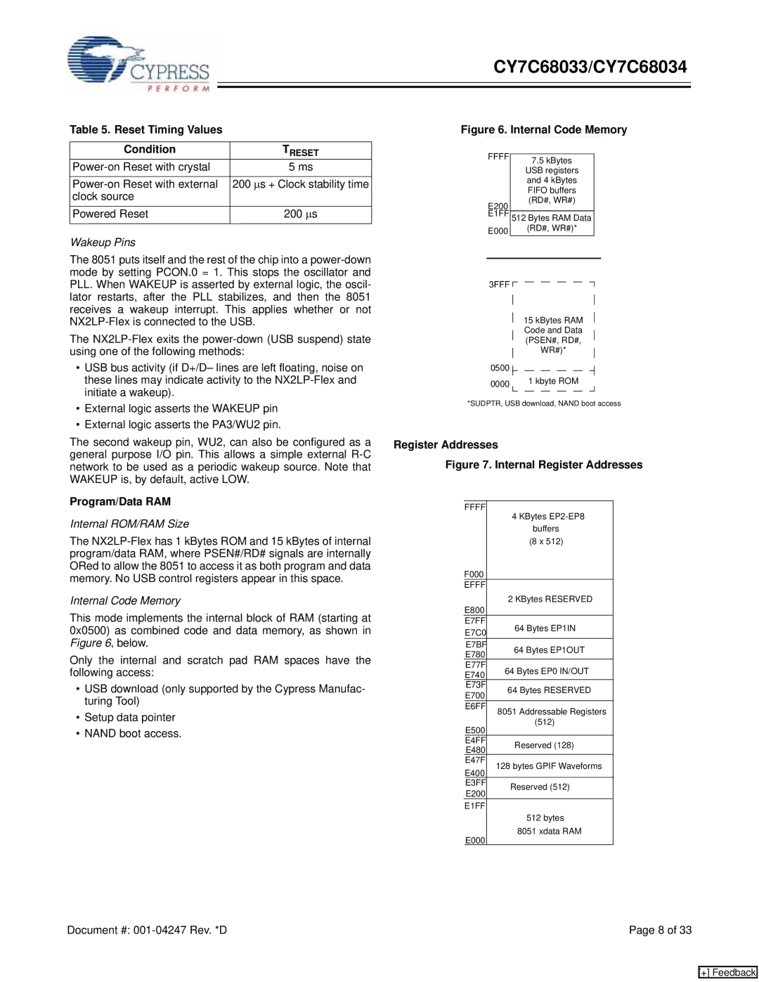
Internal Code Memory
This mode implements the internal block of RAM (starting at 0x0500) as combined code and data memory, as shown in Figure 6, below.
Only the internal and scratch pad RAM spaces have the following access:
•USB download (only supported by the Cypress Manufac- turing Tool)
•Setup data pointer
•NAND boot access.
Figure 6. Internal Code Memory
FFFF |
|
|
7.5 kBytes |
| |
|
| |
| USB registers |
|
| and 4 kBytes |
|
| FIFO buffers |
|
E200 | (RD#, WR#) |
|
|
| |
E1FF | 512 Bytes RAM Data |
|
E000 | (RD#, WR#)* |
|
|
| |
|
|
|
3FFF |
|
|
|
|
|
|
|
|
|
|
|
|
| 15 kBytes RAM |
| ||||||||||
|
| |||||||||||
|
|
| ||||||||||
|
|
| ||||||||||
|
|
| ||||||||||
|
|
| ||||||||||
|
|
| ||||||||||
|
| Code and Data |
| |||||||||
|
|
| ||||||||||
|
|
| (PSEN#, RD#, |
| ||||||||
|
|
|
| |||||||||
0500 |
|
|
| WR#)* |
| |||||||
|
|
|
| |||||||||
|
|
|
|
|
|
|
|
|
|
|
| |
|
|
|
|
|
|
|
|
|
|
|
| |
0000 |
|
| 1 kbyte ROM |
| ||||||||
|
|
| ||||||||||
|
|
| ||||||||||
|
|
|
|
|
|
|
|
|
|
|
|
|
*SUDPTR, USB download, NAND boot access
Register Addresses
Figure 7. Internal Register Addresses
| FFFF | 4 KBytes |
|
| |
|
| buffers |
|
| (8 x 512) |
| F000 |
|
| EFFF |
|
| E800 | 2 KBytes RESERVED |
|
| |
| E7FF | 64 Bytes EP1IN |
| E7C0 | |
|
| |
| E7BF | 64 Bytes EP1OUT |
| E780 | |
|
| |
| E77F | 64 Bytes EP0 IN/OUT |
| E740 | |
|
| |
| E73F | 64 Bytes RESERVED |
| E700 | |
|
| |
| E6FF | 8051 Addressable Registers |
|
| |
| E500 | (512) |
|
| |
| E4FF | Reserved (128) |
| E480 | |
|
| |
| E47F | 128 bytes GPIF Waveforms |
| E400 | |
|
| |
| E3FF | Reserved (512) |
| E200 | |
|
| |
| E1FF |
|
|
| 512 bytes |
| E000 | 8051 xdata RAM |
|
|
Document #: | Page 8 of 33 |
[+] Feedback