CY7C68033/CY7C68034

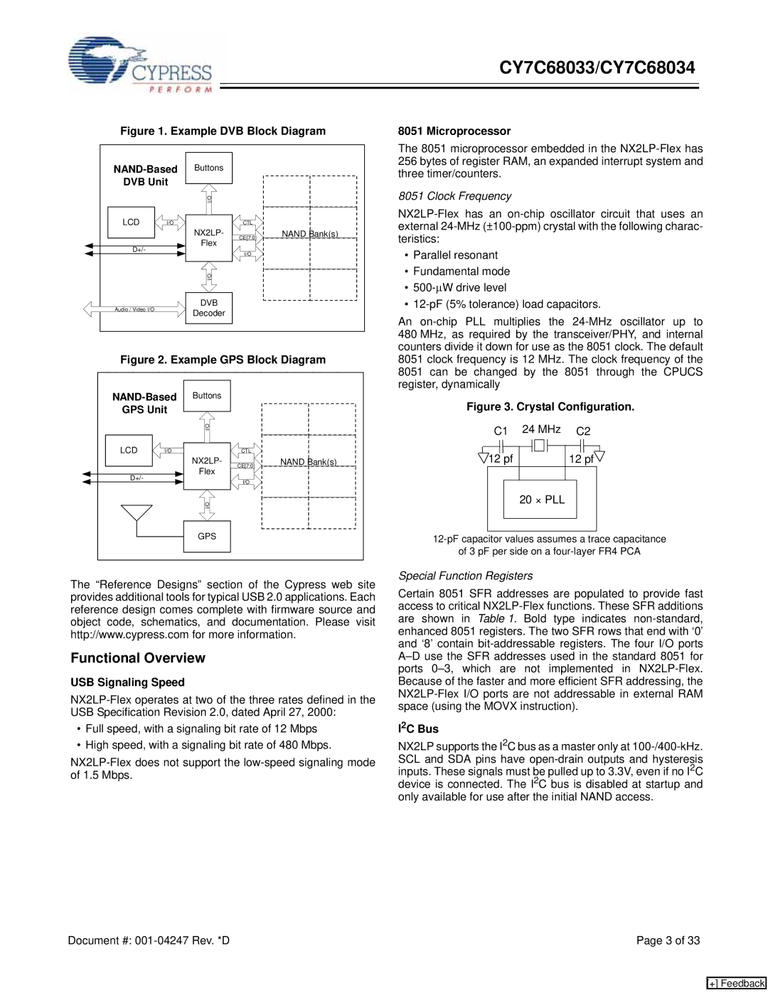
Figure 1. Example DVB Block Diagram

8051 Microprocessor

NAND-Based

DVB Unit

LCD

I/O

D+/-

Audio / Video I/O

Buttons

I/O

NX2LP-

Flex

I/O

DVB

Decoder

CTL


CE[7:0]

NAND Bank(s)

I/O


The 8051 microprocessor embedded in the NX2LP-Flex has 256 bytes of register RAM, an expanded interrupt system and three timer/counters.

8051 Clock Frequency

NX2LP-Flex has an on-chip oscillator circuit that uses an external 24-MHz (±100-ppm) crystal with the following charac- teristics:

Parallel resonant

Fundamental mode

500-μW drive level

12-pF (5% tolerance) load capacitors.

An on-chip PLL multiplies the 24-MHz oscillator up to 480 MHz, as required by the transceiver/PHY, and internal counters divide it down for use as the 8051 clock. The default

Figure 2. Example GPS Block Diagram

8051 clock frequency is 12 MHz. The clock frequency of the 8051 can be changed by the 8051 through the CPUCS register, dynamically

NAND-Based

GPS Unit

LCD

I/O

D+/-

Buttons

I/O

NX2LP-

Flex

I/O

GPS

CTL


CE[7:0]

NAND Bank(s)

I/O


Figure 3. Crystal Configuration.

C1 24 MHz C2


12


pf


12


pf


20 × PLL

12-pF capacitor values assumes a trace capacitance

of 3 pF per side on a four-layer FR4 PCA

The “Reference Designs” section of the Cypress web site provides additional tools for typical USB 2.0 applications. Each reference design comes complete with firmware source and object code, schematics, and documentation. Please visit http://www.cypress.com for more information.

Functional Overview

USB Signaling Speed

NX2LP-Flex operates at two of the three rates defined in the USB Specification Revision 2.0, dated April 27, 2000:

Full speed, with a signaling bit rate of 12 Mbps

High speed, with a signaling bit rate of 480 Mbps.

NX2LP-Flex does not support the low-speed signaling mode of 1.5 Mbps.

Document #: 001-04247 Rev. *D

Special Function Registers

Certain 8051 SFR addresses are populated to provide fast access to critical NX2LP-Flex functions. These SFR additions are shown in Table 1. Bold type indicates non-standard, enhanced 8051 registers. The two SFR rows that end with ‘0’ and ‘8’ contain bit-addressable registers. The four I/O ports A–D use the SFR addresses used in the standard 8051 for ports 0–3, which are not implemented in NX2LP-Flex. Because of the faster and more efficient SFR addressing, the NX2LP-Flex I/O ports are not addressable in external RAM space (using the MOVX instruction).

I2C Bus

NX2LP supports the I2C bus as a master only at 100-/400-kHz. SCL and SDA pins have open-drain outputs and hysteresis inputs. These signals must be pulled up to 3.3V, even if no I2C device is connected. The I2C bus is disabled at startup and only available for use after the initial NAND access.

Page 3 of 33

[+] Feedback

Page 3
Image 3
Cypress CY7C68034 manual Functional Overview, Clock Frequency, USB Signaling Speed, Special Function Registers, I2C Bus