CY7C68033/CY7C68034
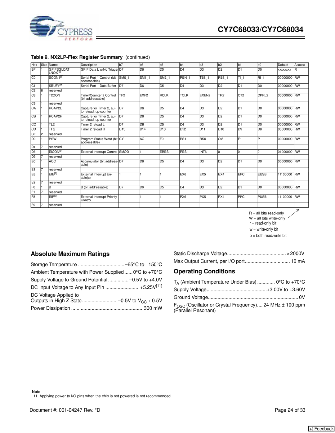
Table 9. NX2LP-Flex Register Summary (continued)
Hex | Size | Name | Description | b7 | b6 | b5 | b4 | b3 | b2 | b1 | b0 | Default | Access |
BF | 1 | GPIFSGLDAT | GPIF Data L w/No Trigger | D7 | D6 | D5 | D4 | D3 | D2 | D1 | D0 | xxxxxxxx | R |
|
| LNOX[9] |
|
|
|
|
|
|
|
|
|
|
|
C0 | 1 | SCON1[9] | Serial Port 1 Control (bit | SM0_1 | SM1_1 | SM2_1 | REN_1 | TB8_1 | RB8_1 | TI_1 | RI_1 | 00000000 | RW |
|
|
| addressable) |
|
|
|
|
|
|
|
|
|
|
C1 | 1 | SBUF1[9] | Serial Port 1 Data Buffer | D7 | D6 | D5 | D4 | D3 | D2 | D1 | D0 | 00000000 | RW |
C2 | 6 | reserved |
|
|
|
|
|
|
|
|
|
|
|
C8 | 1 | T2CON | Timer/Counter 2 Control | TF2 | EXF2 | RCLK | TCLK | EXEN2 | TR2 | CT2 | CPRL2 | 00000000 | RW |
|
|
| (bit addressable) |
|
|
|
|
|
|
|
|
|
|
C9 | 1 | reserved |
|
|
|
|
|
|
|
|
|
|
|
CA | 1 | RCAP2L | Capture for Timer 2, au- | D7 | D6 | D5 | D4 | D3 | D2 | D1 | D0 | 00000000 | RW |
|
|
|
|
|
|
|
|
|
|
|
|
| |
CB | 1 | RCAP2H | Capture for Timer 2, au- | D7 | D6 | D5 | D4 | D3 | D2 | D1 | D0 | 00000000 | RW |
|
|
|
|
|
|
|
|
|
|
|
|
| |
CC | 1 | TL2 | Timer 2 reload L | D7 | D6 | D5 | D4 | D3 | D2 | D1 | D0 | 00000000 | RW |
CD | 1 | TH2 | Timer 2 reload H | D15 | D14 | D13 | D12 | D11 | D10 | D9 | D8 | 00000000 | RW |
CE | 2 | reserved |
|
|
|
|
|
|
|
|
|
|
|
D0 | 1 | PSW | Program Status Word (bit | CY | AC | F0 | RS1 | RS0 | OV | F1 | P | 00000000 | RW |
|
|
| addressable) |
|
|
|
|
|
|
|
|
|
|
D1 | 7 | reserved |
|
|
|
|
|
|
|
|
|
|
|
D8 | 1 | EICON[9] | External Interrupt Control | SMOD1 | 1 | ERESI | RESI | INT6 | 0 | 0 | 0 | 01000000 | RW |
D9 | 7 | reserved |
|
|
|
|
|
|
|
|
|
|
|
E0 | 1 | ACC | Accumulator (bit address- | D7 | D6 | D5 | D4 | D3 | D2 | D1 | D0 | 00000000 | RW |
|
|
| able) |
|
|
|
|
|
|
|
|
|
|
E1 | 7 | reserved |
|
|
|
|
|
|
|
|
|
|
|
E8 | 1 | EIE[9] | External Interrupt En- | 1 | 1 | 1 | EX6 | EX5 | EX4 | EI²C | EUSB | 11100000 | RW |
|
|
| able(s) |
|
|
|
|
|
|
|
|
|
|
E9 | 7 | reserved |
|
|
|
|
|
|
|
|
|
|
|
F0 | 1 | B | B (bit addressable) | D7 | D6 | D5 | D4 | D3 | D2 | D1 | D0 | 00000000 | RW |
F1 | 7 | reserved |
|
|
|
|
|
|
|
|
|
|
|
F8 | 1 | EIP[9] | External Interrupt Priority | 1 | 1 | 1 | PX6 | PX5 | PX4 | PI²C | PUSB | 11100000 | RW |
|
|
| Control |
|
|
|
|
|
|
|
|
|
|
F9 | 7 | reserved |
|
|
|
|
|
|
|
|
|
|
|
R = all bits
W = all bits
w =
b = both read/write bit
Absolute Maximum Ratings
Storage Temperature | ||
Ambient Temperature with Power Supplied | ......0°C to +70°C | |
Supply Voltage to Ground Potential | ||
DC Input Voltage to Any Input Pin | +5.25V[11] | |
DC Voltage Applied to |
|
|
Outputs in High Z State | ||
Power Dissipation | 300 mW | |
Static Discharge Voltage | > 2000V |
Max Output Current, per I/O port | 10 mA |
Operating Conditions |
|
TA (Ambient Temperature Under Bias) | 0°C to +70°C |
Supply Voltage | +3.00V to +3.60V |
Ground Voltage | 0V |
FOSC (Oscillator or Crystal Frequency).... | 24 MHz ± 100 ppm |
(Parallel Resonant) |
|
Note
11. Applying power to I/O pins when the chip is not powered is not recommended.
Document #: | Page 24 of 33 |
[+] Feedback