|
|
|
|
|
|
| CY7C68033/CY7C68034 |
|
|
|
|
|
|
| |
|
|
|
|
|
|
|
|
|
|
|
|
|
|
|
|
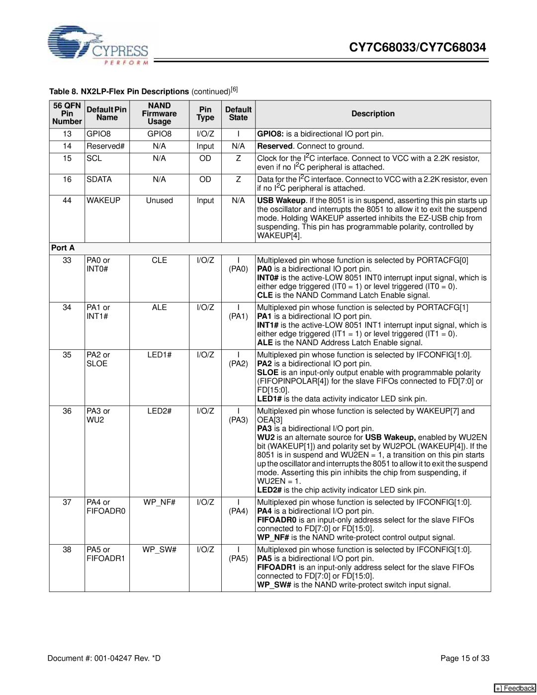
Table 8. |
| ||||||
56 QFN | Default Pin | NAND | Pin | Default | Description | ||
Pin | Name | Firmware | Type | State | |||
Number | Usage |
| |||||
|
|
|
| ||||
13 | GPIO8 | GPIO8 | I/O/Z | I | GPIO8: is a bidirectional IO port pin. | ||
|
|
|
|
|
|
| |
14 | Reserved# |
| N/A | Input | N/A | Reserved. Connect to ground. | |
15 | SCL |
| N/A | OD | Z | Clock for the I2C interface. Connect to VCC with a 2.2K resistor, | |
|
|
|
|
|
|
| even if no I2C peripheral is attached. |
16 | SDATA |
| N/A | OD | Z | Data for the I2C interface. Connect to VCC with a 2.2K resistor, even | |
|
|
|
|
|
|
| if no I2C peripheral is attached. |
44 | WAKEUP | Unused | Input | N/A | USB Wakeup. If the 8051 is in suspend, asserting this pin starts up | ||
|
|
|
|
|
|
| the oscillator and interrupts the 8051 to allow it to exit the suspend |
|
|
|
|
|
|
| mode. Holding WAKEUP asserted inhibits the |
|
|
|
|
|
|
| suspending. This pin has programmable polarity, controlled by |
|
|
|
|
|
|
| WAKEUP[4]. |
Port A |
|
|
|
|
|
|
|
33 | PA0 or |
| CLE | I/O/Z | I | Multiplexed pin whose function is selected by PORTACFG[0] | |
| INT0# |
|
|
|
| (PA0) | PA0 is a bidirectional IO port pin. |
|
|
|
|
|
|
| INT0# is the |
|
|
|
|
|
|
| either edge triggered (IT0 = 1) or level triggered (IT0 = 0). |
|
|
|
|
|
|
| CLE is the NAND Command Latch Enable signal. |
34 | PA1 or |
| ALE | I/O/Z | I | Multiplexed pin whose function is selected by PORTACFG[1] | |
| INT1# |
|
|
|
| (PA1) | PA1 is a bidirectional IO port pin. |
|
|
|
|
|
|
| INT1# is the |
|
|
|
|
|
|
| either edge triggered (IT1 = 1) or level triggered (IT1 = 0). |
|
|
|
|
|
|
| ALE is the NAND Address Latch Enable signal. |
35 | PA2 or | LED1# | I/O/Z | I | Multiplexed pin whose function is selected by IFCONFIG[1:0]. | ||
| SLOE |
|
|
|
| (PA2) | PA2 is a bidirectional IO port pin. |
|
|
|
|
|
|
| SLOE is an |
|
|
|
|
|
|
| (FIFOPINPOLAR[4]) for the slave FIFOs connected to FD[7:0] or |
|
|
|
|
|
|
| FD[15:0]. |
|
|
|
|
|
|
| LED1# is the data activity indicator LED sink pin. |
36 | PA3 or | LED2# | I/O/Z | I | Multiplexed pin whose function is selected by WAKEUP[7] and | ||
| WU2 |
|
|
|
| (PA3) | OEA[3] |
|
|
|
|
|
|
| PA3 is a bidirectional I/O port pin. |
|
|
|
|
|
|
| WU2 is an alternate source for USB Wakeup, enabled by WU2EN |
|
|
|
|
|
|
| bit (WAKEUP[1]) and polarity set by WU2POL (WAKEUP[4]). If the |
|
|
|
|
|
|
| 8051 is in suspend and WU2EN = 1, a transition on this pin starts |
|
|
|
|
|
|
| up the oscillator and interrupts the 8051 to allow it to exit the suspend |
|
|
|
|
|
|
| mode. Asserting this pin inhibits the chip from suspending, if |
|
|
|
|
|
|
| WU2EN = 1. |
|
|
|
|
|
|
| LED2# is the chip activity indicator LED sink pin. |
37 | PA4 or | WP_NF# | I/O/Z | I | Multiplexed pin whose function is selected by IFCONFIG[1:0]. | ||
| FIFOADR0 |
|
|
|
| (PA4) | PA4 is a bidirectional I/O port pin. |
|
|
|
|
|
|
| FIFOADR0 is an |
|
|
|
|
|
|
| connected to FD[7:0] or FD[15:0]. |
|
|
|
|
|
|
| WP_NF# is the NAND |
38 | PA5 or | WP_SW# | I/O/Z | I | Multiplexed pin whose function is selected by IFCONFIG[1:0]. | ||
| FIFOADR1 |
|
|
|
| (PA5) | PA5 is a bidirectional I/O port pin. |
|
|
|
|
|
|
| FIFOADR1 is an |
|
|
|
|
|
|
| connected to FD[7:0] or FD[15:0]. |
|
|
|
|
|
|
| WP_SW# is the NAND |
Document #: | Page 15 of 33 |
[+] Feedback
