|
|
|
|
|
|
|
|
| CY7C68033/CY7C68034 |
| ||
|
|
|
|
|
|
|
|
|
| |||
|
|
|
|
|
|
|
|
|
|
|
|
|
|
|
|
|
|
|
|
|
|
|
|
|
|
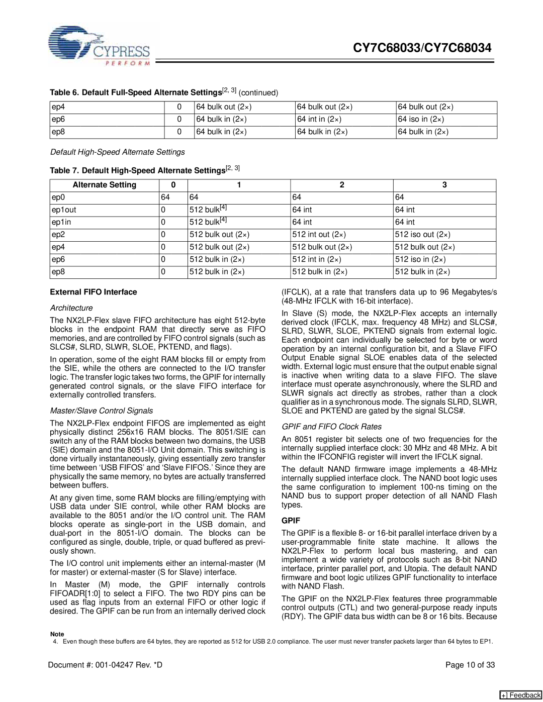
Table 6. Default |
|
|
|
|
|
| ||||||
ep4 |
|
| 0 |
| 64 bulk out (2×) |
| 64 bulk out (2×) |
|
| 64 bulk out (2×) |
| |
|
|
|
|
|
|
|
|
|
|
|
| |
ep6 |
|
| 0 |
| 64 bulk in (2×) |
| 64 int in (2×) |
|
| 64 iso in (2×) |
| |
|
|
|
|
|
|
|
|
|
|
|
| |
ep8 |
|
| 0 |
| 64 bulk in (2×) |
| 64 bulk in (2×) |
|
| 64 bulk in (2×) |
| |
|
|
|
|
|
|
|
|
|
|
| ||
Default |
|
|
|
|
|
|
|
| ||||
Table 7. Default |
|
|
|
|
|
| ||||||
Alternate Setting |
| 0 | 1 | 2 |
| 3 |
| |||||
ep0 |
| 64 | 64 | 64 |
| 64 |
| |||||
|
|
|
|
|
|
|
| |||||
ep1out |
| 0 | 512 bulk[4] | 64 int |
| 64 int |
| |||||
ep1in |
| 0 | 512 bulk[4] | 64 int |
| 64 int |
| |||||
ep2 |
| 0 | 512 bulk out (2×) | 512 int out (2×) |
| 512 iso out (2×) |
| |||||
|
|
|
|
|
|
|
| |||||
ep4 |
| 0 | 512 bulk out (2×) | 512 bulk out (2×) |
| 512 bulk out (2×) |
| |||||
|
|
|
|
|
|
|
| |||||
ep6 |
| 0 | 512 bulk in (2×) | 512 int in (2×) |
| 512 iso in (2×) |
| |||||
|
|
|
|
|
|
|
| |||||
ep8 |
| 0 | 512 bulk in (2×) | 512 bulk in (2×) |
| 512 bulk in (2×) |
| |||||
|
|
|
|
|
|
|
|
|
|
|
|
|
External FIFO Interface
Architecture
The
In operation, some of the eight RAM blocks fill or empty from the SIE, while the others are connected to the I/O transfer logic. The transfer logic takes two forms, the GPIF for internally generated control signals, or the slave FIFO interface for externally controlled transfers.
Master/Slave Control Signals
The
At any given time, some RAM blocks are filling/emptying with USB data under SIE control, while other RAM blocks are available to the 8051 and/or the I/O control unit. The RAM blocks operate as
The I/O control unit implements either an
In Master (M) mode, the GPIF internally controls FIFOADR[1:0] to select a FIFO. The two RDY pins can be used as flag inputs from an external FIFO or other logic if desired. The GPIF can be run from an internally derived clock
Note
(IFCLK), at a rate that transfers data up to 96 Megabytes/s
In Slave (S) mode, the
GPIF and FIFO Clock Rates
An 8051 register bit selects one of two frequencies for the internally supplied interface clock: 30 MHz and 48 MHz. A bit within the IFCONFIG register will invert the IFCLK signal.
The default NAND firmware image implements a
GPIF
The GPIF is a flexible 8- or
The GPIF on the
4. Even though these buffers are 64 bytes, they are reported as 512 for USB 2.0 compliance. The user must never transfer packets larger than 64 bytes to EP1.
Document #: | Page 10 of 33 |
[+] Feedback