Bit | 7 |
| 6 | 5 | 4 | 3 | 2 | 1 | 0 |
|
|
|
|
|
|
|
|
| |
Base + 2h | DI7 |
| DI6 | DI5 | DI4 | DI3 | DI2 | DI1 | DI0 |
Base + 3h | DI15 |
| DI14 | DI13 | DI12 | DI11 | DI10 | DI9 | DI8 |
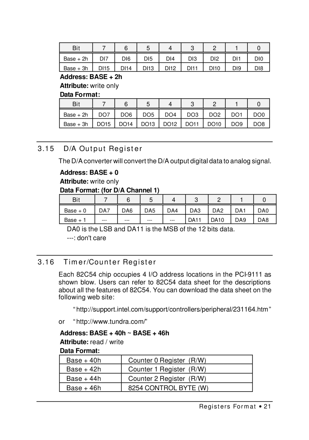
Address: BASE + 2h |
|
|
|
|
|
| |||
Attribute: write only |
|
|
|
|
|
|
| ||
Data Format: |
|
|
|
|
|
|
| ||
Bit | 7 |
| 6 | 5 | 4 | 3 | 2 | 1 | 0 |
|
|
|
|
|
|
|
|
| |
Base + 2h | DO7 |
| DO6 | DO5 | DO4 | DO3 | DO2 | DO1 | DO0 |
Base + 3h | DO15 |
| DO14 | DO13 | DO12 | DO11 | DO10 | DO9 | DO8 |
3.15D/A Output Register
The D/A converter will convert the D/A output digital data to analog signal.
Address: BASE + 0
Attribute: write only
Data Format: (for D/A Channel 1)
Bit | 7 | 6 | 5 | 4 | 3 | 2 | 1 | 0 |
|
|
|
|
|
|
|
|
|
Base + 0 | DA7 | DA6 | DA5 | DA4 | DA3 | DA2 | DA1 | DA0 |
Base + 1 | DA11 | DA10 | DA9 | DA8 |
DA0 is the LSB and DA11 is the MSB of the 12 bits data.
3.16Timer/Counter Register
Each 82C54 chip occupies 4 I/O address locations in the
“http://support.intel.com/support/controllers/peripheral/231164.htm”
or “http://www.tundra.com/”
Address: BASE + 40h ~ BASE + 46h
Attribute: read / write
Data Format:
Base + 40h | Counter 0 Register (R/W) |
Base + 42h | Counter 1 Register (R/W) |
Base + 44h | Counter 2 Register (R/W) |
Base + 46h | 8254 CONTROL BYTE (W) |